- Catalogs
- ROHM Semiconductor
- BD9F500QUZ
BD9F500QUZ
1 /58Pages

BD9F500QUZ
1 /58Pages
Catalog excerpts

Nano Pulse ControlTM 4.5 V to 36 V Input, 5 A Integrated MOSFET Single Synchronous Buck DC/DC Converter BD9F500QUZ Key Specifications General Description BD9F500QUZ is a synchronous buck DC/DC converter with built-in low on-resistance power MOSFETs. It is capable of providing current up to 5 A. It features fast transient response due to Constant On-Time control system. The Light Load Mode control improves efficiency in light-load conditions. It is ideal for reducing standby power consumption of equipment. Power Good function makes it possible for system to control sequence. It achieves the high power density and offer a small footprint on the PCB by employing small package. Input Voltage Range: 4.5 V to 36 V Output Voltage Range: 0.6 V to 14 V Output Current: 5 A (Max) Switching Frequency: 600 kHz, 1 MHz, 2.2 MHz (Typ) High-Side FET ON Resistance: 40 mΩ (Typ) Low-Side FET ON Resistance: 22 mΩ (Typ) Shutdown Current: 2 μA (Typ) Operating Quiescent Current: 20 μA (Typ) Single Synchronous Buck DC/DC Converter Constant On-Time Control Light Load Mode Control Adjustable Soft Start Power Good Output Nano Pulse Control™ Output Capacitor Discharge Function Over Voltage Protection (OVP) Over Current Protection (OCP) Short Circuit Protection (SCP) Thermal Shutdown Protection (TSD) Under Voltage Lockout Protection (UVLO) VMMP16LZ3030 Package Backside Heat Dissipation, 0.5 mm Pitch Applications Step-down Power Supply for SoC, FPGA, Microprocessor Printer (MFP / LBP / IJP / POS) OA Equipment Laptop PC USB Type-C Applications Typical Application Circuit BD9F500QUZ EN PGD VOUT PGND Nano Pulse Control™ is a trademark or a registered trademark of ROHM Co., Ltd. 〇Product structure : Silicon integrated circuit www.rohm.com © 2020 ROHM Co., Ltd. All rights reserved. TSZ22111 • 14 • 001 〇This product has no designed protection against rad
Open the catalog to page 1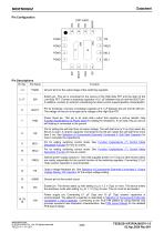
Switch pin. This pin is connected to the source of the High-Side FET and the drain of the Low-Side FET. Connect a bootstrap capacitor of 0.1 µF between this pin and the BOOT pin. In addition, connect an inductor considering the direct current superimposition characteristic. Pin for bootstrap. Connect a bootstrap capacitor of 0.1 µF between this pin and the SW pin. The voltage of this pin is the gate drive voltage of the High-Side FET. Power Good pin. This pin is an open drain output that requires a pull-up resistor. See Function Explanations (4) Power Good for setting the resistance. If not used,...
Open the catalog to page 2
BD9F500QUZ Block Diagram VREG 11 Control Logic VREG ZX/ROCP FREQ www.rohm.com © 2020 ROHM Co., Ltd. All rights reserved. TSZ22111 • 15 • 001
Open the catalog to page 3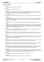
VREF This block generates the internal reference voltage. REG This block generates the internal power supply. Soft Start The Soft Start circuit slows down the rise of output voltage during start-up and controls the current, which allows the prevention of output voltage overshoot and inrush current. The internal soft start time is 2 ms (Typ) when the SS pin is open. A capacitor connected to the SS pin makes the rising time more than 2 ms. Error Amplifier The Error Amplifier adjusts the Main Comparator input voltage to make the internal reference voltage equal to FB voltage. Main Comparator The...
Open the catalog to page 4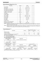
BD9F500QUZ Absolute Maximum Ratings (Ta = 25 °C) Parameter Input Voltage SW Voltage (3 ns pulse width) SW Voltage (30 ns pulse width) Voltage from GND to BOOT Voltage from SW to BOOT VREG Voltage Output Current Maximum Junction Temperature Storage Temperature Range Caution 1: Operating the IC over the absolute maximum ratings may damage the IC. The damage can either be a short circuit between pins or an open circuit between pins and the internal circuitry. Therefore, it is important to consider circuit protection measures, such as adding a fuse, in case the IC is operated over the absolute maximum...
Open the catalog to page 5
BD9F500QUZ Recommended Operating Conditions Parameter Operating Temperature Output Current Output Voltage Setting Input Voltage IOUT VOUT (Note 1) Tj must be 150 °C or less under the actual operating environment. Life time is derated at junction temperature greater than 125 °C. (Note 2) The maximum value of the output current is determined by the control mode selection. (Note 3) The switching frequency is reduced as needed to always ensure a proper regulation at low duty and high duty cycles. Use under the condition of VOUT ≤ VIN × 0.8 [V]. Electrical Characteristics (Unless otherwise specified...
Open the catalog to page 6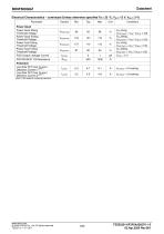
BD9F500QUZ Electrical Characteristics – continued (Unless otherwise specified Ta = 25 °C, VIN = 12 V, VEN = 3 V) Parameter Protection Low-Side FET Over Current (Note 1) Detection Current 1 Low-Side FET Over Current (Note 1) Detection Current 2 Power Good Power Good Rising Threshold Voltage Power Good Falling Threshold Voltage Power Fault Rising Threshold Voltage Power Fault Falling Threshold Voltage PGD Output Leakage Current Conditions VFB rising, VPGDTHGR = VFB / VFBTH x 100 VFB falling, VPGDTHGF = VFB / VFBTH x 100 VFB rising, VPGDTHFR = VFB / VFBTH x 100 VFB falling, VPGDTHFF = VFB / VFBTH...
Open the catalog to page 7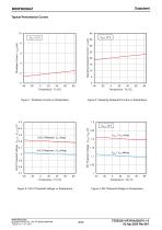
BD9F500QUZ Typical Performance Curves 40 Operating Quiescent Current : IQ [μA] Shutdown Current : ISDN [μA] Figure 1. Shutdown Current vs Temperature Figure 2. Operating Quiescent Current vs Temperature EN Threshold Voltage : VENH, VENL [V] UVLO Threshold Voltage : VUVLO1, VUVLO2 [V] UVLO Release ( VIN rising) 4.2 4.1 UVLO Detection ( VIN falling) 4 3.9 3.8 3.7 Figure 3. UVLO Threshold Voltage vs Temperature www.rohm.com © 2020 ROHM Co., Ltd. All rights reserved. TSZ22111 • 15 • 001 Figure 4. EN Threshold Voltage vs Temperature
Open the catalog to page 8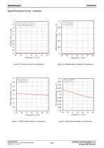
BD9F500QUZ Typical Performance Curves – continued 2 VREG Shutdown Voltage : VVREG_SD [V] Figure 5. EN Input Current vs Temperature Figure 6. VREG Shutdown Voltage vs Temperature 0.608 FB Threshold Voltage : VFBTH [V] 5.35 VREG Output Voltage : VVREG [V] Figure 7. VREG Output Voltage vs Temperature www.rohm.com © 2020 ROHM Co., Ltd. All rights reserved. TSZ22111 • 15 • 001 Figure 8. FB Threshold Voltage vs Temperature
Open the catalog to page 9All ROHM Semiconductor catalogs and technical brochures
 PSR series
17 Pages
 Microcontrollers
32 Pages
 Speech Synthesis LSI Series
20 Pages
 Next-Generation Op Amp series
12 Pages
 LED
LED18 Pages
 Diodes
30 Pages
 Intelligent Power Modules
3 Pages
 Full SiC Power Modules
3 Pages
 SiC Schottky Barrier Diodes
4 Pages
 Microcontroller
13 Pages
 Audio & Video
11 Pages
 Sensors & MEMS
4 Pages
 LED Drivers
4 Pages
 Power Management
36 Pages
 Data Converter
2 Pages
 Clocks & Timers
2 Pages
 Memory
6 Pages
 Motor Drivers
44 Pages
 Power Device Catalog
36 Pages
 CSL1501RW
9 Pages
 UT6JC5 -60V Pch+Pch Power MOSFET
14 Pages
 SH8JB5 -40V Pch+Pch Power MOSFET
14 Pages
 CSL1104WBx Series (x=A/B/C/D)
11 Pages
 RGW00TS65CHR
15 Pages
 RGW80TS65CHR
15 Pages
 RGW60TS65CHR
15 Pages
 QH8KC5
14 Pages
 QH8KC6
14 Pages
 QH8KB5
14 Pages
 QH8KB6
14 Pages
 SH8KC6
14 Pages
 SH8KC7
14 Pages
 SH8KB6
14 Pages
 SH8KB7
14 Pages
 QH8MB5
22 Pages
 SH8MB5
22 Pages
 BM1390GLV-Z
31 Pages
 RPMD-0100
5 Pages
 Short Form Catalog
308 Pages
 EMARMOUR Technology
4 Pages
 Industrial Motor Solutions
40 Pages
 General-purpse ICs
40 Pages
 IPD
IPD4 Pages
 Quick Buck Booster®
6 Pages
 SOT-23 Package Products
4 Pages
 DC/DC Converter Selection Guide
40 Pages
 Linear Regulator Selection Guide
32 Pages
 Sensing Networks Catalog
11 Pages
 Power Solutions Catalog
9 Pages
 Power Management
11 Pages
 Motor Drivers
36 Pages
 Automotive Product Catalog
124 Pages
 EV solutions
8 Pages


Archived catalogs

- Single-pole switch
- Technology switch
- Diode
- Transistor module
- Industrial DC/DC converter module
- SMD DC-DC converter
- ERLO board-mount resistor
- ERLO power resistor
- Switching transistor
- High-speed diode
- Motor driver
- MOSFET transistor
- Power converter
- SMT diode
- Current rectifier
- Bipolar transistor
- ERLO thin-film resistor
- Switching DC-DC converter
- Step-down DC-DC converter