- Catalogs
- ROHM Semiconductor
- Automotive Excellent EMI Characteristics Input/Output Rail-to-Rail CMOS Operational Amplifier
Automotive Excellent EMI Characteristics Input/Output Rail-to-Rail CMOS Operational Amplifier
1 /28Pages

Automotive Excellent EMI Characteristics Input/Output Rail-to-Rail CMOS Operational Amplifier
1 /28Pages
Catalog excerpts

Operational Amplifier Automotive Excellent EMI Characteristics Input/Output Rail-to-Rail CMOS Operational Amplifier BD87581YG-C General Description BD87581YG-C, BD87582YFVM-C and BD87584YFV-C are input/output Rail-to-Rail CMOS operational amplifier. An operating voltage range is wide with 4 V to 14 V. This operational amplifier is the most suitable for automotive requirements such as sensor amplifier, engine control unit, electric power steering, anti-lock braking system and so on because it has features of high slew rate and low input bias current. Furthermore, they have the advantage of EMI tolerance. It makes easier replacing with conventional products or simpler designing EMI. ◼ Operating Supply Voltage Range Single Supply: Dual Supply: ◼ Operating Temperature Range: ◼ Slew Rate: ◼ Input Offset Current: ◼ Input Bias Current: EMARMOURTM Series AEC-Q100 Qualified(Note 1) Input/Output Rail-to-Rail Low Supply Current Wide Operating Supply Voltage Range High Open Loop Voltage Gain Engine Control Unit Electric Power Steering (EPS) Anti-lock Braking System (ABS) Automotive Electronics Typical Application Circuit CF = 10 pF EMARMOURTM is a trademark or a registered trademark of ROHM Co., Ltd. cProduct structure : Silicon integrated circuit www.rohm.com © 2019 ROHM Co., Ltd. All rights reserved. TSZ22111 • 14 • 001 〇This product has no designed protect
Open the catalog to page 1
www.rohm.com © 2019 ROHM Co., Ltd. All rights reserved. TSZ22111 • 15 • 001
Open the catalog to page 2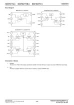
OPAMP: This block is a Rail-to-Rail output operational amplifier with class-AB input / output circuit and differential input stage. Iref: This block supplies reference current which is needed to operate OPAMP block. www.rohm.com © 2019 ROHM Co., Ltd. All rights reserved. TSZ22111 • 15 • 001
Open the catalog to page 3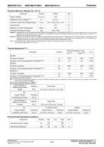
Absolute Maximum Ratings (Ta = 25 °C) Parameter Maximum Junction Temperature Storage Temperature Range Input Current Common-mode Input Voltage Range Differential Input Voltage(Note 1) Supply Voltage Caution 1: Operating the IC over the absolute maximum ratings may damage the IC. The damage can either be a short circuit between pins or an open circuit between pins and the internal circuitry. Therefore, it is important to consider circuit protection measures, such as adding a fuse, in case the IC is operated over the absolute maximum ratings. Caution 2: Should by any chance the maximum junction...
Open the catalog to page 4
Function Explanation 1. EMARMOURTM EMARMOURTM is the brand name given to ROHM products developed by leveraging proprietary technologies covering layout, process, and circuit design to achieve ultra-high noise immunity that limits output voltage fluctuation to ±300 mV or less across the entire noise frequency band during noise evaluation testing under the international ISO11452-2 standard. This unprecedented noise immunity reduces design load while improving reliability by solving issues related to noise in the development of vehicle electrical systems. www.rohm.com © 2019 ROHM Co., Ltd. All rights...
Open the catalog to page 5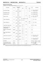
Electrical Characteristics ○BD87581YG-C (Unless otherwise specified VDD = 5 V, VSS = 0 V) Parameter Temperature Range 25 °C Input Offset Voltage Input Offset Current Absolute value Input Bias Current Absolute value Supply Current 25 °C Output Voltage High Common-mode Input Voltage Range Large Signal Voltage Gain Common-mode Rejection Ratio Power Supply Rejection Ratio Output Source Current(Note 1) Output Sink Current(Note 1) Slew Rate Gain Bandwidth Product Total Harmonic Distortion + Noise VOUT = VDD - 0.4 V Absolute value VOUT = VSS + 0.4 V Absolute value (Note 1) Consider the power dissipation...
Open the catalog to page 6
Electrical Characteristics - continued ○BD87582YFVM-C (Unless otherwise specified VDD = 5 V, VSS = 0 V) Parameter Temperature Range 25 °C Input Offset Voltage Input Offset Current Absolute value Input Bias Current Absolute value Supply Current 25 °C Output Voltage High Common-mode Input Voltage Range Large Signal Voltage Gain Common-mode Rejection Ratio Power Supply Rejection Ratio Output Source Current(Note 1) Output Sink Current(Note 1) Slew Rate Gain Bandwidth Product Total Harmonic Distortion + Noise Channel Separation VOUT = VDD - 0.4 V Absolute value VOUT = VSS + 0.4 V Absolute value RL...
Open the catalog to page 7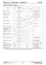
Electrical Characteristics - continued ○BD87584YFV-C (Unless otherwise specified VDD = 5 V, VSS = 0 V) Parameter Temperature Range 25 °C Input Offset Voltage Input Offset Current Absolute value Input Bias Current Absolute value Supply Current 25 °C Output Voltage High Common-mode Input Voltage Range Large Signal Voltage Gain Common-mode Rejection Ratio Power Supply Rejection Ratio Output Source Current(Note 1) Output Sink Current(Note 1) Slew Rate Gain Bandwidth Product Total Harmonic Distortion + Noise Channel Separation VOUT = VDD - 0.4 V Absolute value VOUT = VSS + 0.4 V Absolute value RL...
Open the catalog to page 8
Typical Performance Curves VSS = 0 V Supply Voltage: VDD [V] Figure 1. Supply Current vs Supply Voltage Figure 2. Supply Current vs Ambient Temperature Output Voltage High: VOH [V] Output Voltage High: VOH [V] Figure 3. Output Voltage High vs Supply Voltage (RL = 10 kΩ, VOH = VDD - VOUT) Figure 4. Output Voltage High vs Ambient Temperature (RL = 10 kΩ, VOH = VDD - VOUT) (Note) The above data are measurement value of typical sample; it is not guaranteed. www.rohm.com © 2019 ROHM Co., Ltd. All rights reserved. TSZ22111 • 15 • 001
Open the catalog to page 9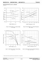
Typical Performance Curves - continued VSS = 0 V Figure 5. Output Voltage Low vs Supply Voltage (RL = 10 kΩ) Figure 6. Output Voltage Low vs Ambient Temperature (RL = 10 kΩ) Output Source Current: IOH [mA] Output Source Current: IOH [mA] Output Voltage: VOUT [V] Figure 7. Output Source Current vs Output Voltage (VDD = 5 V) Figure 8. Output Source Current vs Ambient Temperature (VOUT = VDD - 0.4 V) (Note) The above data are measurement value of typical sample; it is not guaranteed. www.rohm.com © 2019 ROHM Co., Ltd. All rights reserved. TSZ22111 • 15 • 001
Open the catalog to page 10
Typical Performance Curves - continued VSS = 0 V Output Sink Current: IOL [mA] Output Sink Current: IOL [mA] Output Voltage: VOUT [V] Figure 9. Output Sink Current vs Output Voltage (VDD = 5 V) Figure 10. Output Sink Current vs Ambient Temperature (VOUT = VSS + 0.4 V) Input Offset Voltage: VIO [mV] Input Offset Voltage: VIO [mV] Figure 11. Input Offset Voltage vs Supply Voltage (VICM = VDD/2, EK = -VDD/2) Figure 12. Input Offset Voltage vs Ambient Temperature (VICM = VDD/2, EK = -VDD/2) (Note) The above data are measurement value of typical sample; it is not guaranteed. www.rohm.com © 2019 ROHM...
Open the catalog to page 11All ROHM Semiconductor catalogs and technical brochures
 PSR series
17 Pages
 Microcontrollers
32 Pages
 Speech Synthesis LSI Series
20 Pages
 Next-Generation Op Amp series
12 Pages
 LED
LED18 Pages
 Diodes
30 Pages
 Intelligent Power Modules
3 Pages
 Full SiC Power Modules
3 Pages
 SiC Schottky Barrier Diodes
4 Pages
 Microcontroller
13 Pages
 Audio & Video
11 Pages
 Sensors & MEMS
4 Pages
 LED Drivers
4 Pages
 Power Management
36 Pages
 Data Converter
2 Pages
 Clocks & Timers
2 Pages
 Memory
6 Pages
 Motor Drivers
44 Pages
 Power Device Catalog
36 Pages
 CSL1501RW
9 Pages
 UT6JC5 -60V Pch+Pch Power MOSFET
14 Pages
 SH8JB5 -40V Pch+Pch Power MOSFET
14 Pages
 CSL1104WBx Series (x=A/B/C/D)
11 Pages
 BD9F500QUZ
58 Pages
 RGW00TS65CHR
15 Pages
 RGW80TS65CHR
15 Pages
 RGW60TS65CHR
15 Pages
 QH8KC5
14 Pages
 QH8KC6
14 Pages
 QH8KB5
14 Pages
 QH8KB6
14 Pages
 SH8KC6
14 Pages
 SH8KC7
14 Pages
 SH8KB6
14 Pages
 SH8KB7
14 Pages
 QH8MB5
22 Pages
 SH8MB5
22 Pages
 BM1390GLV-Z
31 Pages
 RPMD-0100
5 Pages
 Short Form Catalog
308 Pages
 EMARMOUR Technology
4 Pages
 Industrial Motor Solutions
40 Pages
 General-purpse ICs
40 Pages
 IPD
IPD4 Pages
 Quick Buck Booster®
6 Pages
 SOT-23 Package Products
4 Pages
 DC/DC Converter Selection Guide
40 Pages
 Linear Regulator Selection Guide
32 Pages
 Sensing Networks Catalog
11 Pages
 Power Solutions Catalog
9 Pages
 Power Management
11 Pages
 Motor Drivers
36 Pages
 Automotive Product Catalog
124 Pages
 EV solutions
8 Pages


Archived catalogs

- Single-pole switch
- DC-DC converter
- Technology switch
- Diode
- Transistor module
- Industrial DC/DC converter module
- SMD DC-DC converter
- ERLO board-mount resistor
- ERLO power resistor
- Switching transistor
- High-speed diode
- Motor driver
- MOSFET transistor
- Power converter
- SMT diode
- Current rectifier
- Bipolar transistor
- ERLO thin-film resistor
- Switching DC-DC converter
- Step-down DC-DC converter