
- Catalogs
- ROHM Semiconductor
- 3.5 V to 40 V Input, 1 A Single 2.2 MHz Buck DC/DC Converter For Automotive BD9P1x5MUF-C Serie

- Company
- Products
- Catalogs
- News & Trends
- Exhibitions
3.5 V to 40 V Input, 1 A Single 2.2 MHz Buck DC/DC Converter For Automotive BD9P1x5MUF-C Serie

3.5 V to 40 V Input, 1 A Single 2.2 MHz Buck DC/DC Converter For Automotive BD9P1x5MUF-C Serie
Catalog excerpts
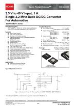
Nano Pulse ControlTM 3.5 V to 40 V Input, 1 A Single 2.2 MHz Buck DC/DC Converter For Automotive BD9P1x5MUF-C Series General Description BD9P1x5MUF-C Series are current mode synchronous buck DC/DC converter integrating POWER MOSFETs. Input Voltage Range: 3.5 V to 40 V (Initial startup is 4.0 V or more) Output Voltage Range BD9P105MUF-C: 0.8 V to 8.5 V BD9P135MUF-C: 3.3 V (Typ) BD9P155MUF-C: 5.0 V (Typ) Output Current: OCP_SEL = L 0.5 A (Max) OCP_SEL = H 1.0 A (Max) Switching Frequency: 2.2 MHz (Typ) Output Voltage Accuracy: ±1.75 % (-40 °C to +125 °C) Shutdown Current: 2.1 μA (Typ) Operating Temperature Range: -40 °C to +125 °C Nano Pulse ControlTM AEC-Q100 Qualified(Note 1) Minimum ON Pulse 50 ns (Max) Synchronous Buck DC/DC Converter Integrating POWER MOSFETs Soft Start Function Current Mode Control Reset Function Quiescent Current 10 μA (Typ) with 12 V Input to 5.0 V Output Light Load Mode (LLM) Forced Pulse Wide Modulation (PWM) Mode Phase Compensation Included Selectable Spread Spectrum Switching External Synchronization Function Selectable Over Current Protection (OCP) Input Under Voltage Lockout (UVLO) Protection Thermal Shut Down (TSD) Protection Output Over Voltage Protection (OVP) Short Circuit Protection (SCP) Enlarged View Automotive Powered Supplies Consumer Powered Supplies VQFN20FV4040 Wettable Flank Package Typical Application Circuit CBST Figure 1. Application Circuit with Discharge Function (BD9P135MUF-C, BD9P155MUF-C) Nano Pulse ControlTM is a trademark or a registered trademark of ROHM Co., Ltd. 〇Product structure : Silicon integrated circuit . www.rohm.com © 2019 ROHM Co., Ltd. All rights reserved. TSZ22111 • 14 • 001 〇This product has no designed protection against ra
Open the catalog to page 1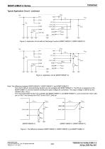
BD9P1x5MUF-C Series Typical Application Circuit - continued CBST RRST VMODE Figure 2. Application Circuit without Discharge Function (BD9P135MUF-C, BD9P155MUF-C) VMODE VSSCG Figure 3. Application Circuit (BD9P105MUF-C) Note: The difference between BD9P105MUF-C, BD9P135MUF-C and BD9P155MUF-C The VOUT_DIS pin and discharge function are not available with BD9P105MUF-C. The FB pin is assigned on the BD9P105MUF-C and the resistors dividing the output voltage are connected. The output voltage is defined by the resistors (RFB1, RFB2). The VOUT discharge function are available with BD9P135MUF-C and BD9P155MUF-C,...
Open the catalog to page 2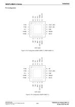
(TOP VIEW) Figure 6. Pin Configuration (BD9P105MUF-C) www.rohm.com © 2019 ROHM Co., Ltd. All rights reserved. TSZ22111 • 15 • 001
Open the catalog to page 3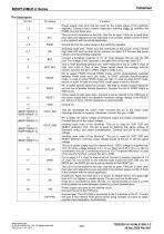
www.rohm.com © 2019 ROHM Co., Ltd. All rights reserved. TSZ22111 • 15 • 001 Function Power supply input pins that are used for the output stage of the switching regulator. Connect input ceramic capacitors referring Page 33 between the PGND pins and these pins. This pin is not connected to the chip. Use this as open. If this pin is used other than open and adjacent pins are expected to be shorted, please confirm if there is any problem with the actual application. Ground pins for the output stage of the switching regulator. Switching node pins. These pins are connected to the source of the internal...
Open the catalog to page 4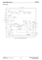
BD9P1x5MUF-C Series Block Diagram VREG tsdout OCP_SEL VREF HOCP Comp Soft Start Control Logic sleep VREF Current Sense Reset PGND VREF VOUT_SNS EN porout uvloout tsdout Figure 7. Block Diagram (BD9P105MUF-C) www.rohm.com © 2019 ROHM Co., Ltd. All rights reserved. TSZ22111 • 15 • 001
Open the catalog to page 5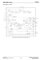
BD9P1x5MUF-C Series Block Diagram - continued VREG tsdout OCP_SEL VREF HOCP Comp Soft Start Control Logic sleep VREF Current Sense VREF Reset PGND VREF EN porout uvloout tsdout Figure 8. Block Diagram (BD9P135MUF-C, BD9P155MUF-C) www.rohm.com © 2019 ROHM Co., Ltd. All rights reserved. TSZ22111 • 15 • 001
Open the catalog to page 6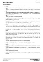
BD9P1x5MUF-C Series Description of Blocks - PreReg This block is the internal power supply for TSD and VREF circuits. VREG This block is the internal power supply circuit. It outputs 3.3 V (Typ) and is the power supply to the control circuit and Driver. TSD This is the thermal shutdown circuit. It will shut down the device when the junction temperature (Tj) reaches to 175 °C (Typ) or more. When the Tj falls below the TSD threshold with hysteresis of 25 °C (Typ), the circuits are automatically restored to normal operation. VREF The VREF block generates the internal reference voltage. POR The POR...
Open the catalog to page 7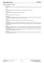
BD9P1x5MUF-C Series Description of Blocks - continued - PWM Comp This block compares the output voltage of the GmAmp2 (Vc) and the saw tooth waveform (Vr) to control the switching duty. Ramp This block generates the saw tooth waveform (Vr) from the clock signal generated by OSC. Control Logic This block controls switching operation and protection functions. Driver This circuit drives the gates of the output FETs. Sleep Comp If output/feedback voltage becomes 101.3 % (Typ) or more, this block puts the device into SLEEP state. This state is released when output/feedback voltage becomes 101.0 %...
Open the catalog to page 8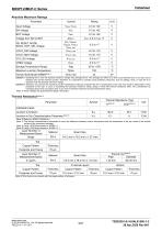
BD9P1x5MUF-C Series Absolute Maximum Ratings Parameter VVIN, VPVIN Input Voltage VOUT_DIS Voltage ΔVBST VFB, VRESET, VMODE, VSSCG VOCP_SEL VVOUT_DIS VOUT_SNS Voltage BST Voltage Voltage from SW to BST FB, RESET, MODE, SSCG, OCP_SEL Voltage VREG Voltage Storage Temperature Range Maximum Junction Temperature Human Body Model (HBM)(Note 1) VCC_EX Voltage Caution 1: Operating the IC over the absolute maximum ratings may damage the IC. The damage can either be a short circuit between pins or an open circuit between pins and the internal circuitry. Therefore, it is important to consider circuit protection...
Open the catalog to page 9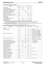
BD9P1x5MUF-C Series Recommended Operating Conditions Parameter VVIN, VPVIN Input Voltage SW Minimum OFF Time (VREG = 3.3 V) SW Minimum OFF Time (VREG = 5.0 V) Operating Temperature Output Current Input Capacitor (VIN Continuous Condition) (Note 3) VREG Capacitor(Note 3) (Note 1) Although the output voltage is configurable at 0.8 V and higher, it may be limited by the SW min ON pulse width. For the same reason, although the output voltage is configurable at 8.5 V and more, it may be limited by the SW minimum OFF pulse width. For the configurable range, please refer to the Output Voltage Setting...
Open the catalog to page 10All ROHM Semiconductor catalogs and technical brochures
 PSR series
17 Pages
 Microcontrollers
32 Pages
 Speech Synthesis LSI Series
20 Pages
 Next-Generation Op Amp series
12 Pages
 LED
LED18 Pages
 Diodes
30 Pages
 Intelligent Power Modules
3 Pages
 Full SiC Power Modules
3 Pages
 SiC Schottky Barrier Diodes
4 Pages
 Microcontroller
13 Pages
 Audio & Video
11 Pages
 Sensors & MEMS
4 Pages
 LED Drivers
4 Pages
 Power Management
36 Pages
 Data Converter
2 Pages
 Clocks & Timers
2 Pages
 Memory
6 Pages
 Motor Drivers
44 Pages
 Power Device Catalog
36 Pages
 CSL1501RW
9 Pages
 UT6JC5 -60V Pch+Pch Power MOSFET
14 Pages
 SH8JB5 -40V Pch+Pch Power MOSFET
14 Pages
 CSL1104WBx Series (x=A/B/C/D)
11 Pages
 BD9F500QUZ
58 Pages
 RGW00TS65CHR
15 Pages
 RGW80TS65CHR
15 Pages
 RGW60TS65CHR
15 Pages
 QH8KC5
14 Pages
 QH8KC6
14 Pages
 QH8KB5
14 Pages
 QH8KB6
14 Pages
 SH8KC6
14 Pages
 SH8KC7
14 Pages
 SH8KB6
14 Pages
 SH8KB7
14 Pages
 QH8MB5
22 Pages
 SH8MB5
22 Pages
 BM1390GLV-Z
31 Pages
 RPMD-0100
5 Pages
 Short Form Catalog
308 Pages
 EMARMOUR Technology
4 Pages
 Industrial Motor Solutions
40 Pages
 General-purpse ICs
40 Pages
 IPD
IPD4 Pages
 Quick Buck Booster®
6 Pages
 SOT-23 Package Products
4 Pages
 DC/DC Converter Selection Guide
40 Pages
 Linear Regulator Selection Guide
32 Pages
 Sensing Networks Catalog
11 Pages
 Power Solutions Catalog
9 Pages
 Power Management
11 Pages
 Motor Drivers
36 Pages
 Automotive Product Catalog
124 Pages
 EV solutions
8 Pages


Archived catalogs

- Single-pole switch
- Technology switch
- Diode
- Transistor module
- Industrial DC/DC converter module
- Board-mount resistor
- Power resistor
- Motor driver
- High-speed diode
- Switching transistor
- SMD DC-DC converter
- MOSFET transistor
- Power converter
- SMT diode
- Current rectifier
- Bipolar transistor
- Thin-film resistor
- Switching DC-DC converter
- Stepper motor driver