- Catalogs
- Rockwell Scientific
- RDX004M4 10 Bit 4 GHz 1:4 Demultiplexer
RDX004M4 10 Bit 4 GHz 1:4 Demultiplexer

RDX004M4 10 Bit 4 GHz 1:4 Demultiplexer
- 10-bit differential input
- 4 GHz operating frequency
- Selectable modes: 1:4, 1:2, 1:1
- Staggered or simultaneous output
- Grey to binary converter
- Selectable DDR clock
- Reset for synchronization
- Pseudo random pattern generator
- LVDS compatible output
- Latency of 3 to 9 clocks depending on mode
- 6 W power dissipation
- BGA package
- Companion chip for RAD004
- RDX004M4-DI: 10 Bit 4 GHz 4:1 DEMUX DIE
- RDX004M4-BG: 10 Bit 4 GHz 4:1 DEMUX, BGA Package
- EVRDX004M4-BG: RDX004M4 Evaluation Board
- Supply Voltages: -0.3 to +0.3 V
- RF Input Voltages: -1 to +1 V
- DC Analog Input Voltages: VEE to +1 V
- DC Digital Input Voltages: -6 to +1 V
- Output Termination Voltages: -2.5 to +3 V
- Temperature: Case -15 to +85 °C, Junction up to +125 °C
- Clock Input Differential Voltage: 200 to 1000 mV
- Clock Input Common Mode: -1.45 to 0.5 V
- Data Input Differential Voltage: 200 to 1000 mV
- Data Input Common Mode: -1.45 to 0.5 V
- Power Supply: VCC 4.75 to 5.25 V, VEE -5.45 to -4.95 V
- Power Dissipation: 6 W
Catalog excerpts

RDX004M4 DATASHEET - PRELIMINARY DS_0136XA1-1309 Teledyne Scientific Company reserves the right to make changes to its product specifications at any time without notice. The information furnished herein is believed to be accurate; however, no responsibility is assumed for its use. RDX004M4 10 Bit 4 GHz 1:4 Demultiplexer Features 10 Bit Differential Input 4 GHz Operating Frequency Selectable 1:4, 1:2, 1:1 Mode Staggered or Simultaneous Output Grey to Binary Converter Selectable DDR clock Reset for multiple device synchronization Pseudo Random Pattern Generator LVDS Compatible Output Latency of 3 to 9 Clocks Depending on Operating Mode 6 W Power Dissipation BGA package Companion Chip for RAD004 Product Description The RDX004M4 was developed as an output demultiplexer for the Teledyne Scientific family of analog to digital converters. Four control signals are used to select features and device operation mode. BIN enables the grey to binary converter. DS0 and DS1 select the demultiplexer mode. It can operate in 1:4, 1:2, and direct mode 1:1. When in demultiplexer mode STAG selects the staggered or simultaneous output. Although the RDX004M4 was developed as a companion chip for the Teledyne Scientific analog to digital converters, it can also be used as a generic demultiplexer. For this application the grey to binary converter can be disabled reducing the power dissipation. Ordering information PART NUMBER DESCRIPTION RDX004M4-DI 10 Bit 4 GHz 4:1 DEMUX DIE RDX004M4-BG 10 Bit 4 GHz 4:1 DEMUX, BGA Package EVRDX004M4-BG RDX004M4 Evaluation Board Figure 1 - Functional Block Diagram
Open the catalog to page 1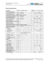
RDX004M4 DATASHEET - PRELIMINARY DS_0136XA1-1309 Teledyne Scientific Company reserves the right to make changes to its product specifications at any time without notice. The information furnished herein is believed to be accurate; however, no responsibility is assumed for its use. Electrical Specification PARAMETER SYMBOL CONDITIONS, NOTES TEST LEVEL MIN TYP MAX UNITS CLOCK INPUT (CLKI(P/N)) Clock Input Differential Voltage VDIFCLKI Differential 200 600 1000 mV Clock Input Common Mode VCMCLKI Differential -1.45 0.5 V Clock Input Resistance RCLK 50 Ù CLOCK OUTPUT (CLKA(P/N), CLKB(P/N), CLKC(P/N),...
Open the catalog to page 3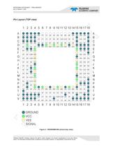
RDX004M4 DATASHEET - PRELIMINARY DS_0136XA1-1309 Teledyne Scientific Company reserves the right to make changes to its product specifications at any time without notice. The information furnished herein is believed to be accurate; however, no responsibility is assumed for its use. Pin Layout (TOP view) Figure 2 - RDX004M4-BG pinout (top view).
Open the catalog to page 5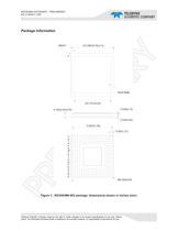
RDX004M4 DATASHEET - PRELIMINARY DS_0136XA1-1309 Teledyne Scientific Company reserves the right to make changes to its product specifications at any time without notice. The information furnished herein is believed to be accurate; however, no responsibility is assumed for its use. Package Information Figure 3 - RDX004M4-BG package, dimensions shown in inches (mm).
Open the catalog to page 6All Rockwell Scientific catalogs and technical brochures
 Track and Hold (T/H) RTH040
16 Pages
 Track and Hold (T/H) RTH030
16 Pages
 Track and Hold (T/H) RTH020
16 Pages
 RTH010 Track and Hold (T/H)
16 Pages
 HMIR
HMIR2 Pages
 CHROMA FPE
2 Pages
 CHROMA FPA
2 Pages
 HxRG
HxRG2 Pages
 TDSO-050
5 Pages
 HAWAII-2RG™
2 Pages


Archived catalogs
 RDA012 12 Bit 1.1 GS/s DAC
11 Pages
 HAWAII 4RG
2 Pages
 UAV-Cam V2M
2 Pages
 UAV-Cam V59M
2 Pages
 UAV-Cam V2M
2 Pages


