- Catalogs
- Rockwell Scientific
- Digital to Analog Converters (DAC) RDA012RZ
Digital to Analog Converters (DAC) RDA012RZ
1 /12Pages

Digital to Analog Converters (DAC) RDA012RZ
1 /12Pages
Catalog excerpts
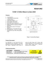
RDA012RZ 12 Bit 1.0 GS/s Return to Zero DAC Features ♦ ♦ ♦ ♦ ♦ ♦ ♦ ♦ ♦ ♦ ♦ 12 Bit Resolution 1 GS/s Minimum Sampling Rate 1.5 GS/s Typical 10 Bit Static Linearity LVDS Compliant Digital Inputs Power Supply: -5.2V, +3.3V Input Code Format: Offset Binary Output Swing: 600 mV @ 50 Ω Termination Reference I/O Pin for Accurate Full-Scale Adjustment Return-to-Zero Output for 2nd Nyquist Operation Differential ECL or Sinusoidal Clock Input Fast settling time: < 1ns 0.1% (+/- 2LSB), switching from code 1536 to 2560 (quarter scale) Figure 1. Functional Block Diagram Product Description The RDA012RZ is a 12-bit GaAs DAC with a data update rate over 1Gsample/s. It has been optimized for ultra-high speed applications. The DAC utilizes a segmented current source to reduce the glitch energy and to achieve high linearity performance. For a flat response at the second Nyquist analog band, a track-andattenuate circuit is integrated. Ordering information PART NUMBER RDA012RZ-QP RDA012RZ-DI EVRDA012RZ-QP DESCRIPTION 12 BIT 1GS/s RZDAC, QFP Package 12 BIT 1GS/s RZDAC, DIE RDA012RZ-QP Evaluation Board The product represented in this datasheet is subject to U.S. Export Law as contained in the International Traffic in Arms Regulations (ITAR) Public Domain Information – Previously Approved for Public Release (DOD Office of Security Review, Case 08-S-0606) Teledyne Scientific Company reserves the right to make changes to its product specifications at any time without notice. The information furnished herein is believed to be accurate; however, no responsibility is assumed for its use.
Open the catalog to page 1
Absolute Maximum Ratings Supply Voltages VEEA, VEED to GNDA …………………….. -0.3V to +0.3V VCC to GNDA …………………………..….… 0 V to +3.8 V Temperature Case Temperature…………………………… -40 to +85 °C Junction Temperature….………………………..….. +125 °C Lead, Soldering (10 Seconds) …………………….. +220 °C Storage….……………………………………… -60 to 125 °C The product represented in this datasheet is subject to U.S. Export Law as contained in the International Traffic in Arms Regulations (ITAR) Public Domain Information – Previously Approved for Public Release (DOD Office of Security Review, Case 08-S-0606) Teledyne Scientific Company reserves...
Open the catalog to page 2
DC Electrical Specification Test Conditions (see notes for specific conditions): Room Temperature; VCC = 3.3V; VEEA = -5.2V; VEED = -5.2V; VREF = -2V; VTT = -2V; TMS = RZ Mode; Clock: 1GHz, 0.6Vpp Differential; Outputs Terminated Into 50 Ω to VCC. PARAMETER 1.0 1.1 1.2 2.0 2.1 3.0 3.1 4.0 4.1 4.2 5.0 5.1 5.2 6.0 6.1 6.2 6.3 6.4 7.0 7.1 8.0 8.1 8.2 8.3 8.4 CONDITIONS, NOTE DC TRANSFER FUNCTION Differential Nonlinearity DNL -0.1 Integral Nonlinearity INL -0.1 TEMPERATURE DRIFT Warm-up Time After Power-up CLOCK INPUT (CLKIP, CLKIN) Input Resistance RCLKI Resistance (CLKI P/N) to VTT 45 50 DATA CLOCK...
Open the catalog to page 3
CONDITIONS, NOTE CLOCK INPUTS (CLKIP, CLKIN) Amplitude VCPP,HCLKI Differential Common Mode Voltage VCCM,HCLKI Maximum Frequency FMAX,HCLKI Minimum Frequency FMIN,HCLKI DATA CLOCK INPUTS (DCLKIP, DCLKIN) Amplitude VDPP Differential Common Mode Voltage VDCM DIGITAL INPUTS (DI<0:11>P, DI<0:11>N) Amplitude VDPP Differential Common Mode Voltage VDCM Data In to DCLKI Setup tDTDKST Both Edges of DCLKI Data In to DCLKI Hold tDTDKHD Both Edges of DCLKI TERMINATION VOLTAGE (VTT) Reference Voltage VTT Termination Voltage for CLKI REFERENCE (VREF) Reference Voltage VREF External Reference POWER SUPPLY REQUIREMENTS...
Open the catalog to page 4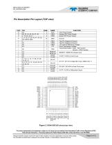
Pin Description Pin Layout (TOP view) NAME VCC VEEA VEED FUNCTION VCC Power Supply Analog VEE Power Supply Digital VEE Power Supply Test Pin: Bypass to Ground Test Pin: Bypass to Ground -2V External Reference Voltage Clock Termination Voltage Track Mode Select: Float – RZ Function Ground – ZOH Function RESETP RESETN CLKIP CLKIN DIP 1 DIN 1 1 1 1 DCLKIP DCLKIN OUTP OUTN RESETP / RESETN Is Reset Input CLKIP / CLKIN Is Clock Input DIP / DIN Is Digital Bit I Input. MSB is Bit 11. DCLKIP / DCLKIN Is Data Clock Input OUTP / OUTN Is Differential Output Figure 2. RDA012RZ-QP pinout (top view). The product...
Open the catalog to page 5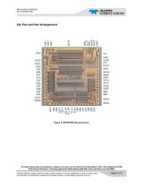
The product represented in this datasheet is subject to U.S. Export Law as contained in the International Traffic in Arms Regulations (ITAR) Public Domain Information – Previously Approved for Public Release (DOD Office of Security Review, Case 08-S-0606) Teledyne Scientific Company reserves the right to make changes to its product specifications at any time without notice. The information furnished herein is believed to be accurate; however, no responsibility is assumed for its use.
Open the catalog to page 6
Theory of Operation The DAC employs MSB segmentation, and the number of bits segmented is carefully chosen for the best compromise between static and dynamic linearity. The 12-bit digital data inputs are latched by a master-slave flip-flop immediately after the input buffer to reduce data skew. MSB data bits are decoded into a thermometer code by a two-stage decoding block, and the LSB data bits are transported through the delay equalizer block. The digital data are synchronized again by a second master-slave flip-flop to reduce the switching glitch. The decoded MSB and LSB data bits drive identical...
Open the catalog to page 7
Signal Description POWER SUPPLIES The RDA012RZ has several power supplies. Their names and uses are defined in the pin description section. Different power supply pins are separated inside the chip, and using separate regulators for each supply is recommended for a good isolation between the digital and analog sections of the chip. No power sequencing is required for reliable operation. Also due to the high-breakdown voltage of the device technology, input may be activated upon an unpowered DAC without damaging the part. which are internally terminated with 50Ω. The VTT pin is the termination...
Open the catalog to page 8All Rockwell Scientific catalogs and technical brochures
 Track and Hold (T/H) RTH040
16 Pages
 Track and Hold (T/H) RTH030
16 Pages
 Track and Hold (T/H) RTH020
16 Pages
 RTH010 Track and Hold (T/H)
16 Pages
 HMIR
HMIR2 Pages
 CHROMA FPE
2 Pages
 CHROMA FPA
2 Pages
 HxRG
HxRG2 Pages
 TDSO-050
5 Pages
 HAWAII-2RG™
2 Pages


Archived catalogs
 RDA012 12 Bit 1.1 GS/s DAC
11 Pages
 HAWAII 4RG
2 Pages
 UAV-Cam V2M
2 Pages
 UAV-Cam V59M
2 Pages
 UAV-Cam V2M
2 Pages


