- Catalogs
- Rockwell Scientific
- Digital to Analog Converters (DAC) RDA012M4
Digital to Analog Converters (DAC) RDA012M4
1 /12Pages

Digital to Analog Converters (DAC) RDA012M4
1 /12Pages
Catalog excerpts

12 Bit Resolution 1.2 GS/s Sampling Rate 4:1 or 2:1 Input Multiplexer Differential Analog Output Input code format: Offset Binary Output Swing: 600 mV with 50 Ω Termination 3.3V NMOS-Compatible Data Inputs Differential ECL or Sinusoidal Clock Input LVDS Compatible Clock Output 10-bit static linearity Reference Output/Input Pin for Accurate Full-Scale Adjustment. 3.3V and -5.2V Power Supply 77 Lead HSD package Figure 1 - Functional Block Diagram Product Description The RDA012M4 is a digital-to-analog converter (DAC) with a 4:1 input multiplexer and a maximum update rate of 1.2GS/s. The integrated DAC utilizes a segmented current source to reduce the glitch energy and to achieve high linearity performance. For best dynamic performance, the DAC outputs are internally terminated with 50Ω resistance, and outputs a nominal full-scale current of 12mA when terminated with external 50Ω resistors. For a convenient interface with most CMOS ICs, the digital data inputs are low voltage NMOS compatible. Ordering information PART NUMBER RDA012M4-HD RDA012M4-DI EVRDA012M4-HD DESCRIPTION 12 BIT 1.2GS/s MUXDAC, HSD Package 12 BIT 1.2GS/s MUXDAC, DIE RDA012M4-HD Evaluation Board Teledyne Scientific Company reserves the right to make changes to its product specifications at any time without notice. The information furnished herein is believed to be accurate; however, no responsibility is assumed for its use.
Open the catalog to page 1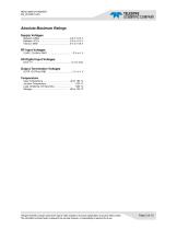
Absolute Maximum Ratings Supply Voltages Between GNDs ………………………….……. -0.3 to +0.3 V Between VCCs …………………..………….. -0.3 to +0.3 V VCCs to GND ………………………..…….… 0 V to +3.8 V RF Input Voltages CLKIP, CLKIN to GND Temperature Case Temperature…………………………… -40 to +85 °C Junction Temperature….……………………..….. +125 °C Lead, Soldering (10 Seconds) ………………….. +220 °C Storage….……………………………..…..… -60 to 125 °C Teledyne Scientific Company reserves the right to make changes to its product specifications at any time without notice. The information furnished herein is believed to be accurate; however, no responsibility...
Open the catalog to page 2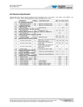
CONDITIONS, NOTE DC TRANSFER FUNCTION Differential Nonlinearity DNL Maximum of Absolute Value Integral Nonlinearity INL Maximum of Absolute Value TEMPERATURE DRIFT Warm-up Time After Power-up HIGH CLOCK INPUT (HCLKIP, HCLKIN) Input Resistance ZCIN Resistance to VTT DIGITAL INPUTS (DIA<0:11>, DIB<0:11>, DIC<0:11>, DID<0:11>) Input Resistance RDIN LOW CLOCK OUTPUT (LCLKOP, LCLKON) Common Mode VCM,LCKO Amplitude Voltage VCPP,LCKO Differential LVDS ANALOG OUTPUTS (OUTP, OUTN) Differential, Terminated Into 50Ω to Full-scale Output Swing VFSD GND on Each Output Single Ended, Terminated Into Full-scale...
Open the catalog to page 3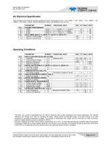
AC Electrical Specification Test Conditions (see notes for specific conditions): Room Temperature; VCC = 3.3V; VEEA = -5.2V; VEED = -5.2V; VREFA = -2V; VREFD = -2V; Clock: 1.2GHz, 0.6Vpp Differential; Outputs Terminated Into 50 Ω to 0V. PARAMETER 10.0 10.1 10.2 10.3 11.0 11.1 11.2 CONDITIONS, NOTE DYNAMIC PERFORMANCE SFDR SFDR 1 FCLK = 800MHz, FOUT = 267MHz SFDR SFDR 2 FCLK = 1GHz, FOUT = 333MHz SFDR SFDR 3 FCLK = 1.2GHz, FOUT = 400MHz DATA TIMING (DIA<0:11>, DIB<0:11>, DIC<0:11>, DID<0:11>) Data In to LCLKO Setup tDTLCKST Data In to LCLKO Hold tDTLCKHD CONDITIONS, NOTE HIGH CLOCK INPUTS (HCLKIP,...
Open the catalog to page 4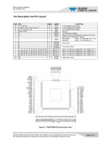
NAME VCC VEEA VEED GND VREFA VREFD VTT HCLKIP HCLKIN LCLKOP LCLKON DIA<0:11> DIB<0:11> DIC<0:11> DID<0:11> OUTP OUTN FUNCTION +3.3V Digital Power Supply -5.2V Analog Power Supply -5.2V Digital Power Supply Ground -2V Reference Voltage Digital Circuitry Bias Reference. Bypass to Ground HCLKI Clock Termination Voltage Mux Mode Float – 4:1 (channels A, B, C, D) Selection: GND – 2:1 (channels B, C) Clock Input Low Clock Output DIA Is Channel A Digital Bit i Input. MSB is bit 11 DIB Is Channel B Digital Bit i Input. MSB is bit 11 DIC Is Channel C Digital Bit i Input. MSB is bit 11 DID Is Channel D...
Open the catalog to page 5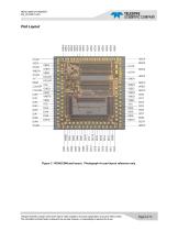
SCIENTIFIC COMPANY
Open the catalog to page 6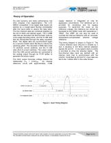
Theory of Operation For best dynamic and static performance, the DAC employs 4-bit segmentation. The 3.3V NMOS compatible 12-bit digital data inputs are latched by a master-slave flip-flop immediately after the input buffer to reduce the data skew. The four-channel data are combined together by the 48:12 MUX and latched again. The 4 MSB data bits are decoded into thermometer code by a two-stage decoding block, and the 8 LSB data bits are transported through the delay equalizer block. The digital data are synchronized again by a second master slave flip-flop to reduce the switching glitch. The...
Open the catalog to page 7
Signal Description HIGH SPEED INPUT CLOCK. The RDA012M4 high-speed clock input is differential and can be driven from typical ECL circuits. Also a differential sinusoidal clock can be used. The HCLKIP and HCLKIN inputs, are internally terminated with 50 Ω to VTT which should be connected to a well decoupled –2.0 volt supply. Since the MUXDAC's output phase noise is directly related to the input clock noise and jitter, a low-jitter clock source is ideal. The internal clock driver generates very little added jitter (~100fs). A 500MHz MUXDAC output demands a white noise induced clock jitter of less...
Open the catalog to page 8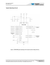
HIGH CLOCK VEEA VEED
Open the catalog to page 9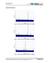
Typical Performance Figure 8 - Output spectrum at Fclk=1200MHz, Fout=340MHz Teledyne Scientific Company reserves the right to make changes to its product specifications at any time without notice. The information furnished herein is believed to be accurate; however, no responsibility is assumed for its use.
Open the catalog to page 10All Rockwell Scientific catalogs and technical brochures
 Track and Hold (T/H) RTH040
16 Pages
 Track and Hold (T/H) RTH030
16 Pages
 Track and Hold (T/H) RTH020
16 Pages
 RTH010 Track and Hold (T/H)
16 Pages
 HMIR
HMIR2 Pages
 CHROMA FPE
2 Pages
 CHROMA FPA
2 Pages
 HxRG
HxRG2 Pages
 TDSO-050
5 Pages
 HAWAII-2RG™
2 Pages


Archived catalogs
 RDA012 12 Bit 1.1 GS/s DAC
11 Pages
 HAWAII 4RG
2 Pages
 UAV-Cam V2M
2 Pages
 UAV-Cam V59M
2 Pages
 UAV-Cam V2M
2 Pages


