RVX5032P
1 /8Pages

RVX5032P
1 /8Pages
Catalog excerpts
rakon g-j-MVoltage Control Crystal Oscillator High performance VCXO in 5 x 3.2 mm Surface Mount Package -jjjjj-duct description The RVX5032P VCXO combines very low RMS phase jitter and low supply current in a small 5 x 3.2 mm SMD package. Available in hundreds of industry standard frequencies from 8 MHz to 800 MHz for fast delivery and reduced inventory levels. Applications • Basestation • Communications • Ethernet • SONET/SDH Features • 0.5 ps integrated RMS phase jitter (12 kHz to 20 MHz) • Fast sample turnaround available • LVCMOS, LVPECL, or LVDS Output options • Wide frequency range • Low power differential outputs • Small form factor 1.3 Rakon Part Number 2.0 FREQUENCY CHARACTERISTICS Line Parameter Test Condition Temperature Range 2.3 Frequency Stability Including Temperature range, Supply variation, Load variation & 2.4 Temperature Stability Temperature range only Unit MHz °C ppm ppm 3.0 POWER SUPPLY Line Parameter 3.1 Supply Voltage (VDD) Test Condition With a tolerance of ±10% With a tolerance of ±5% For LVCMOS For LVPECL For LVDS Value Unit
Open the catalog to page 1
CONTROL VOLTAGE(VCO) Parameter Test Condition Absolute Pull Range (APR) Total Pull Range Control Voltage Linearity Slope Modulation BW Input Impedance Frequency shift from minimum to maximum control voltage Nominal 1.65V Control voltage 0.3 to 3V Positive only Control voltage 0.3 to 3V Value Unit OUTPUT CHARACTERISTICS - LVCMOS UP TO 200MHz ONLY Parameter Output Voltage (Vol) Output Voltage (Voh) Duty Cycle Rise Time / Fall Time RMS Phase Jitter Test Condition 15pF load 15pF load @ 50% VDD 90%/10% at 15 pF output load Typical integrated 12 kHz to 20 MHz Value Unit OUTPUT CHARACTERISTICS...
Open the catalog to page 2
9.0 SSB PHASE NOISE Line Parameter 9.1 SSB Phase Noise Power Density @ 10 Hz Offset 9.2 SSB Phase Noise Power Density @ 100 Hz Offset 9.3 SSB Phase Noise Power Density @ 1 kHz Offset 9.4 SSB Phase Noise Power Density @ 10 kHz Offset 9.5 SSB Phase Noise Power Density @ 100 kHz Offset Value Unit Value Unit Test Condition Typical value for a 155.52 MHz VCXO @ 25°C Typical value for a 155.52 MHz VCXO @ 25°C Typical value for a 155.52 MHz VCXO @ 25°C Typical value for a 155.52 MHz VCXO @ 25°C Typical value for a 155.52 MHz VCXO @ 25°C 10.0 SSB PHASE NOISE Line Parameter Test Condition 10.1...
Open the catalog to page 3
Rakon Product Proposal ENVIRONMENTAL SPECIFICATIONS Mechanical Shock Storage Temperature range Thermal Shock Gross and Fine Leak RoHS Compliant MANUFACTURING INFORMATION Packaging Description Tape and reel. Standard packing quantity is 4000 per reel Solder reflow process as per attached profile
Open the catalog to page 4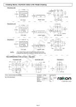
FRONT VIEW TOP VIEW FRONT VIEW NOTE : 1. PIN CONNECTIONS ARE DETAILED IN THE SPECIFICATION. 2. MARKING INFORMATION IS DETAILED IN THE SPECIFICATION. TITLE: XOA/CXO 5032 6-PIN MODEL RELATED DRAWINGS: TOLERANCES: XX = x.x x.xx x.xxx x° Hole = © 2009 Rakon Limited
Open the catalog to page 5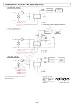
LVPECL TEST CIRCUIT: TITLE: XO/VCXO 6 PIN SERIES TEST CIRCUIT RELATED DRAWINGS: rakon © 2009 Rakon Limited
Open the catalog to page 6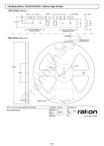
TITLE: XO / VCXO 5032 F SERIES TAPE & REEL RELATED DRAWINGS: TOLERANCES: XX = XX = ±0.1 X.XX = ±0.05 X.XXX = X° = Hole = rakon © 2009 Rakon Limited
Open the catalog to page 7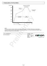
Rakon Product Proposal Drawing Name: Pb-Free Reflow
Open the catalog to page 8All Rakon catalogs and technical brochures
 RTF 1610 RevB
1 Page
 RSX-10v1
1 Page
 RSX-8 v1
1 Page
 LNO100 A4
9 Pages
 RXO7050R
7 Pages
 CIE03
CIE0311 Pages
 CIF0405
8 Pages
 CIF06
CIF069 Pages
 MO G01
3 Pages
 RFPO65
2 Pages
 RFPO60
2 Pages
 RFPO55
2 Pages
 RFPO50
2 Pages
 RFPO45
2 Pages
 RFPO40
2 Pages
 ROX2522S4
2 Pages
 ROX2525S4
2 Pages
 ROX2525T5
2 Pages
 ROX3627T3
2 Pages
 ROX3827T3
2 Pages
 ROX5242T2
2 Pages
 ROX5252T2
2 Pages
 ROX5252T1
2 Pages
 IT3200C
7 Pages
 IT2200J
7 Pages
 IT2200K
7 Pages
 IT2100F
2 Pages
 CFPT9050
9 Pages
 CFPT9000
12 Pages
 CFPT9300
9 Pages
 RFPT500
5 Pages
 RFPT400
5 Pages
 RPT5032N
2 Pages
 RPT7050N
2 Pages
 RPT5032P
2 Pages
 RPT7050P
2 Pages
 RPT5032J
2 Pages
 RPT7050J
2 Pages
 RPT5032A
2 Pages
 RPT7050A
2 Pages
 RHF7050A
2 Pages
 RHT1490J
2 Pages
 RHT1490A
2 Pages
 RFPT100
2 Pages
 RPT7050G
3 Pages
 RFPT200
7 Pages
 RFPT700
6 Pages
 RPT7050D
2 Pages
 RVX1490M
7 Pages
 RVX7050R
8 Pages
 RVX7050P
8 Pages
 RVX7050M
9 Pages
 RVX5032R
8 Pages
 RVX5032M
7 Pages
 RVX2520P
1 Page
 RVX2520R
1 Page
 RVG1490L
2 Pages
 RCV2520Q
1 Page
 RXO7050P
7 Pages
 RXO7050M
9 Pages
 RXO5032R
7 Pages
 RXO5032P
7 Pages
 RXO5032M
10 Pages
 RXO2520P
1 Page
 RXO2520R
1 Page
 RXG1490L
2 Pages
 RCX2520Q
1 Page
 QEN49
QEN494 Pages
 QEN55
QEN554 Pages
 RK115
RK1152 Pages
 CFPX3750
7 Pages
 CFPX3758
7 Pages
 CFPX3000
7 Pages
 RHC-49US
5 Pages
 RSX-5
RSX-55 Pages
 Synchronous Ethernet
2 Pages
 Base Station Solutions
2 Pages
 GNSS Based Synchronisation
2 Pages
 Small Cell Solutions
2 Pages
 The Internet of Things
2 Pages
 GNSS Positioning Solutions
2 Pages
 RGX-3
RGX-37 Pages
 RSX-8
RSX-810 Pages
 RSX10
RSX105 Pages
 RSX-11
5 Pages
 RSX1612
7 Pages
 RXT2520AT
6 Pages
 RXT2016AT
6 Pages
 RTF3215
1 Page
 RK 409
7 Pages
 RK 407
2 Pages
 CIF07
CIF076 Pages
 BASE STATION FACT SHEET
2 Pages
 DEFENSE FACT SHEET
2 Pages
 SMALL CELLS FACT SHEET
2 Pages
 Space OCXO series RK 408
9 Pages
 Crystal filters FTF 1
2 Pages
 Rakon XO QEN79
4 Pages
 ULN USO Module Assembly
5 Pages


- Electronic oscillator
- Surface-mount oscillator
- Frequency oscillator
- OCXO oscillator
- Crystal resonator
- SMD oscillator
- Oscillator for telecom applications
- XO oscillator
- Voltage oscillator
- Phase oscillator
- Power oscillator
- Low-noise oscillator
- Clock oscillator
- Oscillator with connector
- Automated oscillator
- Plug-in oscillator
- High-stability oscillator
- VCO oscillator
- SAW oscillator