- Catalogs
- PRECITEC OPTRONIK
- Measurement of Semiconductor Chips
- Products
- Catalogs
- News & Trends
- Exhibitions
Measurement of Semiconductor Chips
1 /3Pages
Measurement of Semiconductor Chips
1 /3Pages
Catalog excerpts

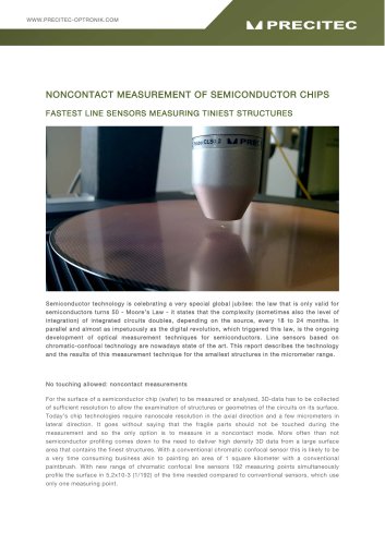
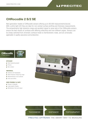
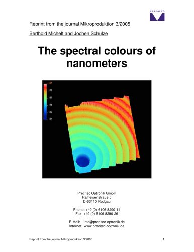
NONCONTACT MEASUREMENT OF SEMICONDUCTOR CHIPS FASTEST LINE SENSORS MEASURING TINIEST STRUCTURES Semiconductor technology is celebrating a very special global jubilee: the law that is only valid for semiconductors turns 50 - Moore’s Law - it states that the complexity (sometimes also the level of integration) of integrated circuits doubles, depending on the source, every 18 to 24 months. In parallel and almost as impetuously as the digital revolution, which triggered this law, is the ongoing development of optical measurement techniques for semiconductors. Line sensors based on chromatic-confocal technology are nowadays state of the art. This report describes the technology and the results of this measurement technique for the smallest structures in the micrometer range. No touching allowed: noncontact measurements For the surface of a semiconductor chip (wafer) to be measured or analysed, 3D-data has to be collected of sufficient resolution to allow the examination of structures or geometries of the circuits on its surface. Today’s chip technologies require nanoscale resolution in the axial direction and a few micrometers in lateral direction. It goes without saying that the fragile parts should not be touched during the measurement and so the only option is to measure in a noncontact mode. More often than not semiconductor profiling comes down to the need to deliver high density 3D data from a large surface area that contains the finest structures. With a conventional chromatic confocal sensor this is likely to be a very time consuming business akin to painting an area of 1 square kilometer with a conventional paintbrush. With new range of chromatic confocal line sensors 192 measuring points simultaneously profile the surface in 5.2x10⁻³ (1/192) of the time needed compared to conventional sensors, which use only one measuring point.
Open the catalog to page 1
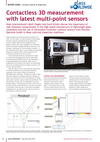
Despite high measurement speed of the line sensors focusing on representative sectors can save even more time. These regions are usually defined by the manufacturing process; but nonetheless, it is most important to receive precise and descriptive results of those areas. Figure1: 3D-Wafer-Topography, measured with a line sensor. The structures are 9 μm high compared to the inner circle area (yellow). The displayed area was scanned in less than a second. © Precitec Optronik The Chromatic-confocal Measurement Principle In their operation chromatic-confocal sensors exploit an optical aberration,...
Open the catalog to page 2
3D-Data within the shortest time The raw data delivered by the sensor can be processed in software to detect periodic patterns and structures. Most frequently used are coded height views to detect faults by observing the height, radii, diameters and gaps in structures. Another display possibility is the height profile, showing a cut through the scanned structure, which can be manipulated in software after the measurement has been made. Figure 3: 2D-Height-view measured by a line sensor with an enlarged section shown to the right. The outer diameter of the circular embankment-like structures (bumps...
Open the catalog to page 3All PRECITEC OPTRONIK catalogs and technical brochures
 CHRocodile MPS 2 L
2 Pages
 CHRomatic Sensors
2 Pages
 Heads
Heads2 Pages
 CHRocodile 2 DPS
2 Pages
 CHRomatic Vision Camera
2 Pages
 Flying Spot Scanner
2 Pages
 Measuring Sensors
2 Pages
 Optical Probes
2 Pages


- Visible imager
- Red Rooster industrial camera
- Full-color camera system
- Image processing camera module
- Red Rooster GigE camera
- Compact imager
- Red Rooster inspection camera
- Additive manufacturing machine
- Thickness gauge
- High-speed camera module
- Portable thickness gauge
- Industrial 3D printer
- Distance sensor
- Measurement monitoring module
- Measurement scanner
- Environmental monitoring system
- Inspection scanner
- Coating thickness gauge
- Production monitoring system
- Online monitoring module