- Catalogs
- PRECITEC OPTRONIK
- Applications Optical Measurement Technologies & Sensors
- Products
- Catalogs
- News & Trends
- Exhibitions
Applications Optical Measurement Technologies & Sensors
1 /5Pages

Applications Optical Measurement Technologies & Sensors
1 /5Pages
Catalog excerpts

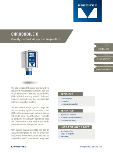
OPTICAL MEASUREMENT TECHNOLOGIES & SENSORS MEASURING PLASTICS Non-destructive measuring of plastic welded seams Welded seams in plastics must often undergo non- destructive tests. This may be the case in medical applications, such as multi-chamber pouches. Also the connection between the pouch and hoses and connectors can also be joined with welded seams. Quality and reproducibility can also be tested by the thickness of the welded seam. Product recommendation: CHRocodile K Measuring the wall thickness of plastic moulded parts Plastic moulded parts, such as cuvettes or pipettes, can be measured without contact with an infrared interferometric measuring system. Wall thicknesses can be determined in this case directly with the optical probe and a spacer on their own if no measuring machine is Product recommendation: CHRocodile K MELI BERi PRAZISE SCHNELL PRECITEC OPTRONIK THE SMART WAY TO MEASURE
Open the catalog to page 1
Measuring the thickness of plastics or plastic coatings Polycarbonates are coated to increase scratch resistance or UV resistance, for example. The coating and the material thickness can be measured by optical sensors without the sensors coming into contact with the items. Polycarbonate, a transparent plastic, is often used as an alternative to glass. Compared with brittle glass, polycarbonate is lighter and considerably more shock- resistant. Its negative properties, such as scratch- resistance or UV resistance can be reduced by coatings. For example, polyurethane acrylate layers of a few microns...
Open the catalog to page 2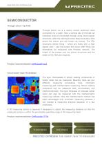
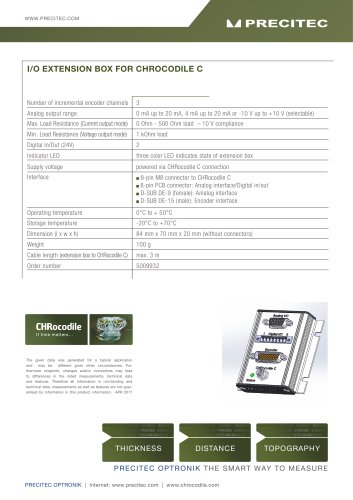
Through silicon via is a mainly vertical electrical metal connection by a wafer. Here a vertical pile of thinned out individual chips is connected through using small copper structures. After the etching process these protrude a little above the silicon and are known as bumps. The TSV structures before filling - which are holes with a high aspect ratio - and the bumps that occur after filling can themselves be measured with Precitec sensors. The height of the bumps over the silicon structures and the depth of the TSVs are required. Product recommendation: CHRocodile CLS Circuit board layer thicknesses...
Open the catalog to page 3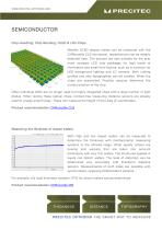
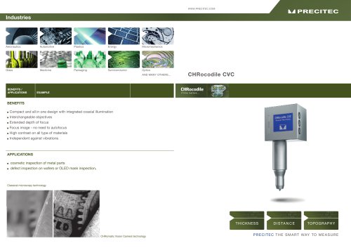
SEMICONDUCTOR Chip-Handling: Chip-Bonding, OLED & LED-Chips Metallic OLED display masks can be measured with the CHRocodile CLS line sensor. Imperfections can be reliably detected here. The sensors are also suitable for the ever more compact LED chip packages for high levels of illumination and small form factors, such as is common for LED background lighting and LC screens. Both cutting profiles and also topographies can be created. When the chips are assembled, Precitec sensors determine the correct position of the chip. Often individual LEDs are no longer used but highly integrated chips with...
Open the catalog to page 4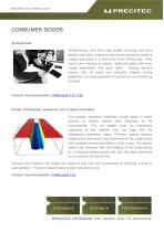
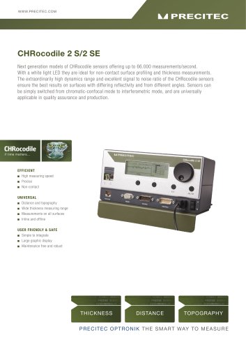
CONSUMER GOODS Smartphones, with their high quality surfaces, and also tablets and other consumer electronics products combine metals and glass in a more and more refined way. Their layers are a mixture of plastic, metal and glass that must merge seamlessly with each other. Optical sensors ensure that all parts are perfectly aligned during assembly. For measurements, the parts do not have to be Product recommendation: CHRocodile 2 S/ 2 SE Screen thicknesses, measuring pits in glass substrates The coated, extremely hardened screen glass in smart phones or tablets places high demands on its workmanship....
Open the catalog to page 5All PRECITEC OPTRONIK catalogs and technical brochures
 CHRocodile MPS 2 L
2 Pages
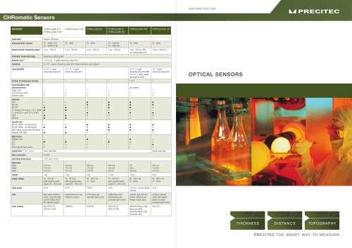
 CHRomatic Sensors
2 Pages
 Heads
Heads2 Pages
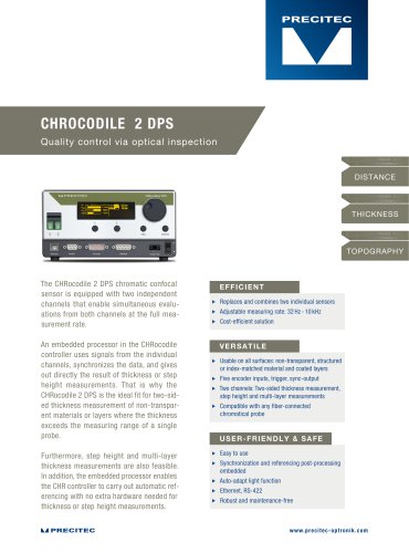 CHRocodile 2 DPS
2 Pages
 CHRomatic Vision Camera
2 Pages
 Flying Spot Scanner
2 Pages
 Measuring Sensors
2 Pages
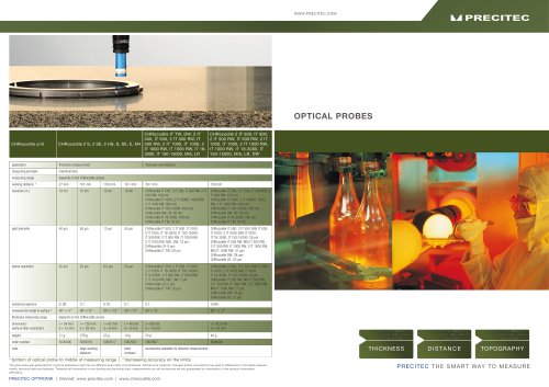
 Optical Probes
2 Pages


- Visible imager
- Red Rooster industrial camera
- Full-color camera system
- Image processing camera module
- Red Rooster GigE camera
- Compact imager
- Red Rooster inspection camera
- Additive manufacturing machine
- Thickness gauge
- High-speed camera module
- Portable thickness gauge
- Industrial 3D printer
- Distance sensor
- Measurement monitoring module
- Measurement scanner
- Environmental monitoring system
- Inspection scanner
- Coating thickness gauge
- Production monitoring system
- Online monitoring module