
- Catalogs
- Power Integrations
- TinySwitch-PK

TinySwitch-PK

TinySwitch-PK
Catalog excerpts
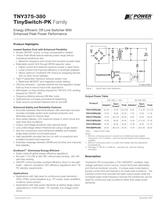
Figure 1. Typical Peak Power Application. 230 VAC 15%85-265 VAC Product > 3 Adapter > 1 OpenFrame > 1 OpenFrame > 2 PeakAdapter > 2 PeakTNY375PN/GN 8.5 W15 W16.5 W6 W11.5 W12.5 W TNY376PN/GN 10 W19 W22 W7 W15 W17 W TNY377PN/GN 13 W23.5 W28 W8 W18 W23 W TNY378PN/GN 16 W28 W34 W10 W21.5 W27 W TNY379PN/GN 18 W32 W39 W12 W25 W31 W TNY380PN/GN 20 W36.5 W45 W14 W28.5 W35 W > Table 1. Output Power Table. Notes: 1. Minimum continuous power in a typical non-ventilated enclosed adapter measured at +50 ѰC ambient. Use of an external heatsink will increase power capability.2. Minimum continuous power in an open frame design (see Key Applications Considerations). 3. Packages: P: DIP-8C, G: SMD-8C. Lead free only. See Part Ordering Information.
Open the catalog to page 1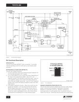
BYPASS/ MULTI-FUNCTION (BP/M) DRAIN (D) REGULATOR 5.85 V BYPASS PIN UNDER-VOLTAGE 1.0 V + V LINE UNDER-VOLTAGE RESET AUTO- RESTART COUNTER 115 A 25 A FAULT PRESENT CURRENT LIMIT COMPARATOR ENABLE > + - BYPASS CAPACITOR SELECT AND CURRENT LIMIT STATE MACHINE 5.85 V 4.9 V SOURCE (S) V > ILIMIT + - JITTER2X CLOCKOSCILLATOR > T DCMAX THERMAL SHUTDOWN ENABLE/ UNDER- VOLTAGE (EN/UV) > S R Q 1.0 V 6.4 V > Q OVP LATCH RESET LEADING EDGE BLANKING > PI-4550-121406 Figure 2 Functional Block Diagram. > PI-4348-111607 Figure 3. Pin Confi guration. >
Open the catalog to page 2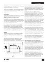
A. When the current out of this pin exceeds the threshold current, a low logic level (disable) is generated at the output of the enable circuit until the current out of this pin is reduced to less than the threshold current. This enable circuit output is sampled at the beginning of each cycle on the rising edge of the clock signal. If high, the power MOSFET is turned on for that cycle (enabled). If low, the power MOSFET remains off (disabled). Since the sampling is done only at the beginning of each cycle, subsequent changes in the EN/UV pin voltage or current during the remainder of the cycle...
Open the catalog to page 3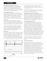
Adaptive Switching Cycle On-Time Extension Adaptive switching cycle on-time extension keeps the cycle on until current limit is reached, instead of prematurely terminating after the DC Over Temperature Protection > The thermal shutdown circuitry senses the die temperature. The threshold is typically set at 142 C with 75 аC hysteresis. When the die temperature rises above this threshold, the power MOSFET is disabled and remains disabled, until the die temperature falls by 75 C, at which point it is re-enabled. A large hysteresis of 75 аC (typical) is provided to prevent overheating of the PC board...
Open the catalog to page 4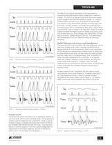
V DRAINV EN CLOCKDCDRAINIMAX > PI-2749-082305 Figure 6. Operation at Near Maximum Loading (f OSC 264 kHz). Figure 7. Operation at Moderately Heavy Loading (f V DRAINV EN CLOCKDCDRAINIMAX V DRAIN V EN CLOCK DC DRAIN I MAX > PI-2667-082305 OSC 264 kHz). PI-4540-050407 Figure 8. Operation at Medium Loading (f OSC 132 kHz).
Open the catalog to page 5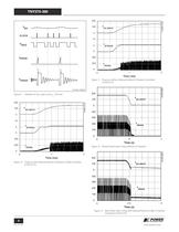
PI-4541-042507 Figure 9. Operation at Very Light Load (f > OSC 132 kHz). VDC-INPUT > PI-2348-030801 VDC-INPUT > PI-4865-101007 VDRAIN VBYPASS > Figure 10. Power-up With Optional External UV Resistor (4 M ) Connected to EN/UV Pin. Figure 11. Power-up Without Optional External UV Resistor Connected to EN/UV Pin. Figure 12. Normal Power-down Timing (Without UV Resistor). Figure 13. Slow Power-down Timing With Optional External (4 M VDC-INPUT > PI-2395-030801 VDRAIN > ) UV Resistor Connected to EN/UV Pin. >
Open the catalog to page 6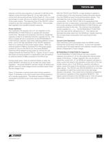
) connected to the EN/UV pin.During power-down, when an external resistor is used, the power MOSFET will switch for 32 ms after the output loses regulation. The power MOSFET will then remain off without any glitches since the undervoltage function prohibits restart when the line voltage is low. Figure 12 illustrates a typical power-down timing waveform. Figure 13 illustrates a very slow power-down timing waveform, as in standby applications. The external resistor (4 M ) is connected from the power supply positive DC input to the EN/UV pin, the power MOSFET switching will be delayed during power-up...
Open the catalog to page 7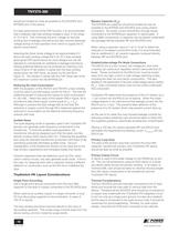
F ceramic capacitor is placed directly between BP and SOURCE pins. F or 10 F to select the reduced or increased current limit mode, it is recommended that an additional 0.1 should be located as close as possible to the SOURCE and BYPASS pins of the device.For best performance of the OVP function, it is recommended that a relatively high bias winding voltage is used, in the range of 15 V-30 V. This minimizes the error voltage on the bias winding due to leakage inductance and also ensures adequate voltage during no-load operation from which to supply the IC device consumption. Selecting the Zener...
Open the catalog to page 10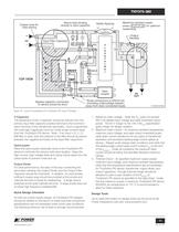
Copper area for heat sinkingReturn bias windingdirectly to input capacitorMaximize hatched copper areas ( ) for optimum heatsinking Safety Spacing > Y1- Capacitor + - > HV Input Filter Capacitor Output Rectifier PRI T r a n s f o r m e r BIAS BIAS R SEC D PRI C > TinySwitch-PK S S S S BP EN/UV > BP Opto- coupler > UV DC OUT + - Bypass capacitor connection to device should be shortRoute connections to EN/UV pin(including undervoltage resistor)away from drain connected traces > PI-4675-051507 Figure 16. Layout Considerations for TinySwitch-PK Using P Package. Y-Capacitor > DS does not exceed 650...
Open the catalog to page 11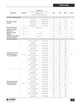
Control Functions (cont.)BP/M Pin Charge Current V > BP/M = 0 V,T I > CH1 J = 25 аCSee Note D, ETNY375-378-8.3-5.4-2.5 V = 4 V,T ATNY379-380-9.7-7.1-3.9I > BP/M CH2 J = 25 CSee Note D, ETNY375-378-5-3.5-1.5TNY379-380-6.6-4.8-2.1 BP/M Pin Voltage V > BP/M See Note D5.65.856.15V BP/M Pin Voltage Hysteresis V > BP/MH 0.800.951.20V BP/M Pin Shunt Voltage V > SHUNT I > BP = 2 mA6.06.46.7V EN/UV Pin Line Under-voltage Threshold I > LUV T > J = 25 аC22.52527.5 A Circuit Protection Peak Current Limit (BP/M Capacitor = 0.1 di/dt = 72 mA/ sT > J = 25 CSee Note FTNY375PN330355380 mATNY375GN330355387di/dt...
Open the catalog to page 13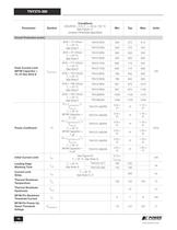
Circuit Protection (cont.) Peak Current Limit (BP/M Capacitor = 10 di/dt = 72 mA/ sT > J = 25 аCSee Note FTNY375PN349375413 mATNY375GN349375424di/dt = 91 mA/ sT > J = 25 CSee Note FTNY376PN465500550TNY376GN465500565di/dt = 117 mA/ sT > J = 25 аCSee Note FTNY377PN665715787TNY377GN665715808di/dt = 143 mA/ I > LIMITPEAKinc F) See Note E sT > J = 25 CSee Note FTNY378PN786845930TNY378GN786845955di/dt = 169 mA/ sT > J = 25 аCSee Note FTNY379PN9079751073TNY379GN9079751102di/dt = 195 mA/ sT > J = 25 CSee Note FTNY380PN102811051216TNY380GN102811051249 > 2 f = I > LIMITPEAK(TYP)2 Зf > 2 OSC(TYP) 2 f I...
Open the catalog to page 14All Power Integrations catalogs and technical brochures
 InnoSwitch3-AQ
28 Pages
 InnoSwitch4-CZ
30 Pages
 LinkSwitch-TNZ
24 Pages
 2SIS0400T2C0C-33
10 Pages
 2SMS0220D2C0C-CM1200DC-34X
8 Pages
 2SML0220D2E0-FF600R17ME4
4 Pages
 2SIL1200T2A0-33
4 Pages
 InnoSwitch3-TN
23 Pages
 ChiPhy
6 Pages
Archived catalogs
 DPA-Switch
34 Pages
 CAPZero
8 Pages
 HiperPLC
26 Pages
 LinkSwitch-TN
20 Pages
 LinkSwitch-II
10 Pages
 HiperPLC
26 Pages
 LinkSwitch-CV
20 Pages
 LinkSwitch-LP
16 Pages
 TinySwitch-III
24 Pages
 TOPSwitch-HX
48 Pages
 PeakSwitch
24 Pages
 PeakSwitch™ Family
4 Pages
- DC power supply
- AC/DC power supply
- Switched-mode power supply
- DC-DC converter
- Diode
- Isolated DC-DC converter
- Transistor module
- SMD capacitor
- High-voltage power supply
- High-speed diode
- SMD DC-DC converter
- MOSFET transistor
- Power converter
- Step-down DC-DC converter
- DC/DC converter for telecom applications
- Printed circuit board power supply
- LED driver
- Adjustable LED driver