
- Catalogs
- Power Integrations
- LinkSwitch-CV

LinkSwitch-CV

LinkSwitch-CV
The LinkSwitch-CV family provides energy-efficient, off-line switchers with precise primary-side constant-voltage (CV) control, eliminating the need for optocouplers and secondary CV control circuitry. This results in simplified CV converter design and tight output voltage regulation.
The output power varies by product and input voltage range. For instance, the LNK623PG/DG delivers 6.5 W at 230 VAC and 5.0 W at 85-265 VAC for adapters, with increased power for open frame designs.
- Eliminates optocoupler and secondary CV control circuitry.
- Self-biasing IC compensates for temperature variations.
- Advanced protection features like auto-restart and thermal shutdown.
- EcoSmart® technology ensures energy efficiency, complying with global regulations.
- Green package: Halogen-free and RoHS compliant.
Applicable in DVDs, set-top boxes, adapters, standby supplies, home appliances, and industrial controls.
The LinkSwitch-CV integrates a high voltage power MOSFET with a power supply controller, using ON/OFF control to regulate output voltage and features like frequency jittering and current limit circuits.
- Auto-restart reduces power during faults.
- Thermal shutdown with automatic recovery.
- Current limit circuit prevents excessive current flow.
A typical application is a three-output, primary-side regulated flyback power supply using the LNK626PG, capable of delivering 7 W continuously and 10 W peak.
- Single point grounding improves surge capabilities.
- Minimize secondary loop area to reduce EMI.
- Provide sufficient copper area for heat dissipation.
A trace is used as one electrode of a spark gap along the isolation barrier, directing ESD energy from the secondary to the primary side AC input. A 10 mil gap is recommended to decouple noise and prevent circuit damage.
Figures illustrate recommended PCB layouts with and without external bias, emphasizing minimizing drain trace area, maximizing copper area for heat sinking, and ensuring feedback resistors are close to the device.
Discusses the use of clamp circuits to manage primary leakage inductance and reduce voltage overshoot, providing component recommendations and configurations for different inductance levels.
For designs with output power ≤5 W, clampless designs are feasible with specific requirements. For higher power, external clamps are necessary.
Explains the impact of diode recovery speed on feedback voltage ringing and output ripple, providing solutions to minimize pulse grouping and improve regulation.
A checklist is provided to verify maximum drain voltage, current, and thermal conditions under worst-case scenarios.
Detailed specifications for control functions, thermal impedance, and circuit protection are provided, including maximum ratings and typical performance characteristics.
Figures illustrate various performance characteristics and test setups for feedback pin measurements.
Includes procedures for adjusting P voltage, measuring VFBth, and testing leakage and breakdown characteristics.
Conforms to JEDEC specification MS-001-AB for standard dual-in-line (DIP) package, with dimensions primarily in inches and millimeter equivalents in parentheses.
Includes LinkSwitch Product Family, CV Series Number, Package Identifier, and options for standard configurations or Tape & Reel for D Package.
Power Integrations reserves the right to make changes to improve reliability or manufacturability, with no warranty provided and all implied warranties disclaimed.
Headquarters in San Jose, CA, USA, with regional offices worldwide and applications hotline and fax available.
Catalog excerpts

* Dramatically Simplifi es CV Converters > ΕՕՕՕՕՕՕՕՕ Օ Eliminates optocoupler and all secondary CV control circuitry Eliminates bias winding supply Ֆ IC is self biasing Advanced Performance Features Compensates for external component temperature variationsVery tight IC parameter tolerances using proprietary trimming technology Continuous and/or discontinuous mode operation for design fl exibilityFrequency jittering greatly reduces EMI fi lter costEven tighter output tolerances achievable with external resistor selection/trimming Advanced Protection/Safety Features EcoSmart Auto-restart protection reduces delivered power by >95% for output short circuit and all control loop faults (open and shorted components) Hysteretic thermal shutdown automatic recovery reduces power supply returns from the fi eld Meets HV creepage requirements between Drain and all other pins, both on the PCB and at the package > Wide RangeHV DC Input DS FBBP LinkSwitch-CV PI-5195-080808 (a) Typical Application Schematic (b) Output Characteristic V O ֱ5% Auto-Restart Ζ Energy Effi cient > PI-5196-080408 I O No-load consumption <200 mW at 230 VAC and down to below 70 mW with optional external bias Easily meets all global energy effi ciency regulations with no added components ON/OFF control provides constant effi ciency down to very light loads ideal for mandatory EISA and ENERGY STAR 2.0 regulationsNo primary or secondary current sense resistors ֖ maximizes effi ciency > Figure 1. Typical Application Schematic (a) and Output Characteristic Envelope (b). Green Package Halogen free and RoHS compliant package > *Optional with LNK623-624PG/DG. (see Key Application Considerations section for clamp and other external circuit design considerations). Applications Output Power Table DVD/STBAdaptersStandby and auxiliary supplies Home appliances, white goods and consumer electronics Industrial controls > 230 VAC 15%85-265 VAC Product 3 Peak or Open Frame Peak or Open Frame Adapter 1 1 2 Adapter 2 LNK623PG/DG 6.5 W9 W5.0 W6 W LNK624PG/DG 7 W11 W5.5 W6.5 W LNK625PG/DG 8 W13.5 W6.5 W8 W LNK626PG 10.5 W17 W8.5 W10 W Table 1. Output Power Table. Based on 5 V Output. Notes: 1. Minimum continuous power in a typical non-ventilated enclosed adapter measured at +50 ѰC ambient. 2. Maximum practical continuous power in an open frame design with adequate heatsinking, measured at 50 C ambient (see Key Application Considerations section for more information). 3. Packages: P: DIP-8C, D: SO-8C. The LinkSwitch-CV dramatically simplifies low power, constant voltage (CV) converter design through a revolutionary control technique which eliminates the need for both an optocoupler and secondary CV control circuitry while providing very tight output voltage regulation. The combination of proprietary IC trimming and E-ShieldЙ transformer construction techniques enables Clampless designs with the LinkSwitch-CV LNK623/4. LinkSwitch-CV provides excellent cross-regulation for multiple-output flyback applications such as DVDs and STBs. A 700 V power MOSFET and ON/OFF control state machine, self-biasing, frequency jittering, cycle-by-cycle current limit, and hysteretic thermal shutdown circuitry are all incorporated onto one IC. > www.powerint.com December 2008 size="-1">
Open the catalog to page 1
s), whilst keeping the disable period of 2.5 seconds. This effectively reduces the Auto-Restart duty cycle to less than 0.01%. > Constant Voltage (CV) Operation > The controller regulates the feedback pin voltage to remain at V Over-Temperature Protection The thermal shutdown circuitry senses the die temperature. The threshold is set at 142 C typical with a 60 аC hysteresis. When the die temperature rises above this threshold (142 C) the power MOSFET is disabled and remains disabled until the die temperature falls by 60 аC, at which point the MOSFET is re-enabled. The LinkSwitch-CV combines a...
Open the catalog to page 3
Single Point Grounding Use a single point (Kelvin) connection at the negative terminal of the input fi lter capacitor for the LinkSwitch-CV SOURCE pin and bias winding return. This improves surge capabilities by returning surge currents from the bias winding directly to the input fi lter capacitor. Bypass Capacitor The BYPASS pin capacitor should be located as close as possible to the SOURCE and BYPASS pins. Feedback Resistors Place the feedback resistors directly at the FEEDBACK pin of the LinkSwitch-CV device. This minimizes noise coupling. Thermal Considerations The copper area connected to...
Open the catalog to page 5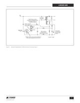
B+ PRI RTN CLAMP > DS FBBP IsourceTraceimpedance Bias winding currents flow in signal source tracesVoltage drops across trace impedance may cause degraded performance Power currentsflow in signal source traceLine surgecurrents can flow through device Drain trace in closeproximity of feedback tracewill couple noise intofeedback signal $ V > S PI-5267-111008 Figure 8. Schematic Representation of Electrical Impact of Improper Layout. >
Open the catalog to page 7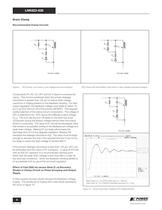
R R > C2 C2 C > C1 C > C1 D > C2 R > C1 R > C1 D > C1 D > C1 PI-5107-110308 PI-5108-110308 Figure 9. RCD Clamp, Low Power or Low Leakage Inductance Designs. RCD Clamp With Zener Bleed. High Power or High Leakage Inductance Designs. > Black Trace: D > C1 is a FR107 (fast type, trr = 500 ns)Gray Trace: D > C1 is a 1N4007G (standard recovery, trr = 2 us) Figure 10. Clamp Circuit (top). Feedback Pin Voltage (bottom). >
Open the catalog to page 8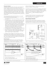
Figure 12. RC Network Across R > BOTTOM (R6) to Reduce Pulse Grouping. Top Trace: Drain Waveform (200 V/div)Bottom Trace: Output Ripple Voltage (50 mV/div)Split Screen with Bottom Screen ZoomTop Trace: Drain Waveform (200 V/div) Bottom Trace: Output Ripple Voltage (50 mV/div) Top Trace: Drain Waveform (200 V/div)Bottom Trace: Output Ripple Voltage (50 mV/div)Split Screen with Bottom Screen ZoomTop Trace: Drain Waveform (200 V/div) Bottom Trace: Output Ripple Voltage (50 mV/div) Figure 11. Not Pulse Grouping (<5 Consecutive Switching Cycles). Pulse Grouping (>5 Consecutive Switching Cycles). >
Open the catalog to page 9All Power Integrations catalogs and technical brochures
 InnoSwitch3-AQ
28 Pages
 InnoSwitch4-CZ
30 Pages
 LinkSwitch-TNZ
24 Pages
 2SIS0400T2C0C-33
10 Pages
 2SMS0220D2C0C-CM1200DC-34X
8 Pages
 2SML0220D2E0-FF600R17ME4
4 Pages
 2SIL1200T2A0-33
4 Pages
 InnoSwitch3-TN
23 Pages
 ChiPhy
6 Pages
Archived catalogs
 DPA-Switch
34 Pages
 CAPZero
8 Pages
 HiperPLC
26 Pages
 LinkSwitch-TN
20 Pages
 LinkSwitch-II
10 Pages
 TinySwitch-PK
24 Pages
 HiperPLC
26 Pages
 LinkSwitch-LP
16 Pages
 TinySwitch-III
24 Pages
 TOPSwitch-HX
48 Pages
 PeakSwitch
24 Pages
 PeakSwitch™ Family
4 Pages
- DC power supply
- AC/DC power supply
- Switched-mode power supply
- DC-DC converter
- Isolated DC-DC converter
- Transistor module
- High-voltage power supply
- SMD capacitor
- High-speed diode
- SMD DC-DC converter
- MOSFET transistor
- Power converter
- Step-down DC-DC converter
- DC/DC converter for telecom applications
- Printed circuit board power supply
- LED driver
- Adjustable LED driver