
- Catalogs
- Power Integrations
- InnoSwitch3-AQ

InnoSwitch3-AQ

InnoSwitch3-AQ
The InnoSwitch3-AQ is a flyback switcher IC for automotive applications, featuring a 750 V and 900 V switch with FluxLink feedback. It offers up to 90% efficiency and supports a wide input voltage range from 30 V to 925 V. The IC is AEC-Q100 qualified and manufactured in IATF16949 certified facilities.
- EcoSmart™ technology for energy efficiency with less than 15 mW no-load power consumption.
- Advanced protection features including auto-restart for output overvoltage protection (OVP) and optional under-voltage (UV) protection.
- Full safety compliance with reinforced isolation and >4000 VAC isolation voltage.
- Green package that is halogen-free and RoHS compliant.
The IC is suitable for auxiliary, standby, and bias power supplies in automotive systems such as traction inverters, DC-DC converters, and on-board chargers.
- Output power varies with input voltage: INN3977CQ provides up to 30 W, while INN3996CQ provides up to 20 W.
- Primary and secondary controllers are integrated into a single IC, allowing for accurate output voltage regulation.
- Multiple protection features including line over/undervoltage protection, output overvoltage, over-current limiting, and over-temperature shutdown.
The InnoSwitch3-AQ combines a high-voltage power MOSFET switch with primary and secondary controllers. It uses FluxLink technology for feedback, enabling accurate voltage and current information transmission. The primary controller operates in various modes and includes features like frequency jitter oscillator, current limit controller, and over-temperature protection. The secondary controller includes a transmitter circuit, constant voltage and current control circuits, and integrated protection features.
- Over-temperature protection with hysteretic or latch-off response.
- Input line voltage monitoring for undervoltage and overvoltage protection.
- Current limit operation with a ramp that adjusts based on load conditions.
- Auto-restart mechanism for fault conditions such as output overload or short-circuit.
The document includes figures illustrating the application schematic, block diagrams of primary and secondary controllers, pin configuration, and a flowchart for primary-secondary handshake.
The document describes the auto-restart mechanism and handshake protocol between primary and secondary controllers in a power supply system. The primary controller enters auto-restart mode under certain conditions, allowing the secondary controller to take over. If the primary stops switching or does not respond to the secondary's cycle requests, a handshake protocol ensures the secondary is ready to assume control.
After power-up recovery from faults or auto-restart events, the primary controller pauses for an auto-restart on-time period (~82 ms) to listen for secondary requests. If two consecutive requests are detected, the primary switches to slave mode; otherwise, it continues under primary control until handshake pulses are received.
The InnoSwitch3-AQ features a noise reduction mode that avoids resonant bands between 7 kHz and 12 kHz by inhibiting the gate drive to the power MOSFET if a secondary switch request occurs within this window.
The secondary controller is powered by a 4.4 V regulator and uses various pins for handshaking, timing, and regulating output voltage and current. It initiates cycle requests with a minimum off-time to ensure energy delivery to the load.
At start-up, the primary controller limits switching frequency and current. The secondary controller ramps up frequency after handshake completion. In case of short-circuits or overloads, the device enters constant-current mode and may auto-restart if voltage thresholds are not met.
The system regulates output voltage and current using feedback and current sense resistors. Overvoltage protection mechanisms include bleed currents and commands to the primary to latch-off or auto-restart.
This mode improves efficiency by forcing switching when the primary switch voltage is minimal in discontinuous conduction mode. It is automatically engaged and disabled based on conduction mode.
The system includes various protection features such as SR disable protection, open SR protection, and feedback pin short detection to ensure safe operation and prevent faults.
An example circuit for a 12 V, 30 W power supply using the INN3977CQ IC is provided, detailing component connections and functions for efficient power conversion and regulation.
The document concludes with considerations for achieving maximum practical continuous output power under specified conditions.
1. Efficiency is assumed to be greater than 89% at the specified power level.
2. Transformer primary inductance has a tolerance of ±10%.
3. Maximum conduction losses are limited to 0.8 W.
4. The component must be board-mounted with SOURCE pins soldered to a sufficient area of copper or a heat sink to maintain a temperature at or below 125 °C.
5. Minimum continuous power is measured in a typical non-ventilated enclosed adapter at 40 °C ambient.
The INN3977CQ IC provides primary-side output overvoltage protection using an internal protection mechanism triggered by a threshold current into the PRIMARY BYPASS pin. A Zener diode, resistor, and blocking diode combination is recommended for effective OVP.
The InnoSwitch3-AQ IC can start in self-powered mode, but a bias winding is required for continuous operation to achieve no-load power consumption below 10 mW.
The secondary-side OVP uses an auto-restart circuit triggered by an input current exceeding a threshold into the SECONDARY BYPASS pin. A Zener diode is used for direct output sensed OVP.
BPP Capacitor: A 0.47 mF or 4.7 mF capacitor is recommended, preferably a multi-layer ceramic capacitor for compact designs.
Bias Winding: A bias winding should provide at least 1 mA to the PRIMARY BYPASS pin, with a turns ratio ensuring 7 V at the lowest load condition.
Primary Sensed OVP: A Zener diode connected to the PRIMARY BYPASS pin can detect secondary overvoltage faults.
Primary-Side Snubber Clamp: An RCD clamp is recommended to prevent voltage spikes.
StackFET Configuration: Used for high input voltages (>550 VDC) to increase breakdown voltage.
SECONDARY BYPASS Pin Capacitor: A 2.2 uF, 10 V / X7R or X5R capacitor is recommended.
SR FET: Use of an SR FET improves efficiency, with specific threshold voltage requirements.
Output Capacitor: Low ESR aluminum electrolytic capacitors are suitable, with 200 mF to 300 mF per ampere of output current.
The document outlines the specifications for the InnoSwitch3-AQ IC, including voltage ratings, feedback circuit requirements, and thermal considerations. Capacitors should have a voltage rating higher than the highest output voltage with sufficient margin. The feedback pin voltage is set at 1.265 V, requiring a voltage divider network to maintain this voltage.
Recommendations for circuit board layout include single-point grounding, placement of bypass capacitors, and minimizing primary loop area. The primary clamp circuit should limit peak voltage on the DRAIN pin using an RCD clamp or Zener diode. Thermal management involves maximizing copper area for heat dissipation.
For EMI reduction, component placement and loop area minimization are crucial. Additional measures include using a small capacitor in parallel with the clamp diode and adjusting SR switch RC snubber components. Transformer design should ensure power delivery at the lowest input voltage, with a KP close to 0.9 recommended.
Switching frequency can be set between 25 kHz to 95 kHz, with 60 kHz recommended for lowest temperature. Reflected output voltage (VOR) should be set to maintain KP = 0.8 at minimum input voltage. The ripple to peak current ratio (KP) should be close to 0.9 for most designs.
Absolute maximum ratings for various pins and conditions are provided, including DRAIN pin voltage and current, storage temperature, and operating junction temperature. Thermal resistance values are also specified.
Verification tests include checking maximum drain voltage and current, and conducting thermal checks to ensure component limits are not exceeded under worst-case conditions.
Catalog excerpts
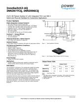
InnoSwitch3-AQ INN3977CQ, INN3996CQ CV/CC QR Flyback Switcher IC with Integrated 750 V and 900 V Switch and FluxLink Feedback for Automotive Applications Product Highlights Highly Integrated, Compact Footprint • Up to 90% efficiency across full load range • Incorporates a multi-mode Quasi-Resonant (QR) / CCM flyback controller, 750 V and 900 V switch and secondary-side sensing • Integrated FluxLink™, HIPOT-isolated, feedback link • Wide input voltage 30 V to 925 V with StackFET™ • AEC-Q100 qualified • Fab, assembly and test site are IATF16949 certified InnoSwitch3-AQ EcoSmart™ – Energy Efficient • Auto-restart fault response for output OVP Optional Current Sense Primary Switch and Controller • Less than 15 mW no-load • Low heat dissipation Advanced Protection / Safety Features Optional Features • Auto-restart output UV protection with option for peak power delivery Figure 1. Typical Application Schematic. Full Safety and Regulatory Compliance • • • • • Reinforced isolation Isolation voltage >4000 VAC 100% production HIPOT testing UL1577 approved and TUV (EN60950) in process Excellent noise immunity enables designs that achieve class “A” performance criteria for EN61000-4 suite; EN61000-4-2, 4-3 (30 V/m), 4-4, 4-5, 4-6, 4-8 (100 A/m) and 4-9 (1000 A/m), FMC1278 (RI-115) Figure 2. High Creepage, Safety-Compliant InSOP-24D Package. Green Package • Halogen free and RoHS compliant • Auxiliary, standby and bias power supplies for automotive used in traction inverter, DC-DC converter and on-board charger Output Power Table Product 2 Description The InnoSwitch™3-AQ family of ICs dramatically simplifies the design and manufacture of flyback power converters, particularly those requiring high efficiency and/or compact size. The InnoSwitch3-AQ family combines primary and secondary controllers and safety-rated feedback into a single IC allowing accurate output voltage regulation even with wide input voltage range of 30 V to 925 V. InnoSwitch3-AQ family devices incorporate multiple protection features including line over and undervoltage protection, output overvoltage and over-current limiting, and over-temperature shutdown for automotive applications. Devices are available with standard and peak power delivery options, and commonly used auto-restart protection behaviors. Table 1. Output Power Table. Notes: 1. Max output power is dependent on the design. With condition that package temperature must be < 125 °C. Uses PCB copper for heat sinking. 2. Package: InSOP-24D. 3. With StackFET. This Product is Covered
Open the catalog to page 1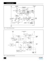
UNDER/OVER INPUT VOLTAGE (V) PRIMARY BYPASS (BPP) PRIMARY BYPASS REGULATOR ENABLE FAULT AUTO-RESTART COUNTER LINE INTERFACE PRIMARY BYPASS PIN CAPACITOR SELECT AND CURRENT LIMIT UV/OV OSCILLATOR/ TIMERS VSHUNT VBP+ From Secondary Controller RECEIVER CONTROLLER Power Switch PRIMARY BYPASS PIN UNDERVOLTAGE THERMAL SHUTDOWN PRIMARY OVP LATCH/ AUTO-RESTART LATCH-OFF/ AUTO-RESTART Figure 3. Primary Controller Block Diagram. SYNC RECTIFIER DRIVE (SR) HANDSHAKE/ AUTO-RESTART CABLE DROP COMPENSATION/ FEEDBACK COMPENSATION tOFF(MIN) OSCILLATOR/ TIMER FEEDBACK DRIVER SECONDARY LATCH/ AUTO-RESTART tSS(RAMP)...
Open the catalog to page 2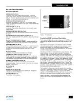
InnoSwitch3-AQ Pin Functional Description Secondary-Side Pins ISENSE (IS) Pin (Pin 1) Connection to the power supply output terminals. An external current sense resistor should be connected between this and the GND pin. If current regulation/accurate over-current protection is not required, this pin should be tied to the GND pin. SECONDARY GROUND (GND) (Pin 2) Ground for the secondary IC. Note this is not the power supply output ground due to the presence of the sense resistor between this and the ISENSE pin. FEEDBACK (FB) Pin (Pin 3) Connection to an external resistor divider to set the power...
Open the catalog to page 3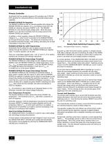
PRIMARY BYPASS Pin Regulator The PRIMARY BYPASS pin has an internal regulator that charges the PRIMARY BYPASS pin capacitor to VBPP by drawing current from the DRAIN pin whenever the power MOSFET is off. The PRIMARY BYPASS pin is the internal supply voltage node. When the power MOSFET is on, the device operates from the energy stored in the PRIMARY BYPASS pin capacitor. In addition, a shunt regulator clamps the PRIMARY BYPASS pin voltage to VSHUNT when current is provided to the PRIMARY BYPASS pin through an external resistor. This allows the InnoSwitch3-AQ to be powered externally through a...
Open the catalog to page 4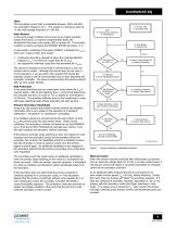
InnoSwitch3-AQ Jitter The normalized current limit is modulated between 100% and 95% at a modulation frequency of fM. This results in a frequency jitter of ~7 kHz with average frequency of ~100 kHz. Auto-Restart In the event a fault condition occurs (such as an output overload, output short-circuit, or external component/pin fault), the InnoSwitch3-AQ enters auto-restart (AR) or latches off. The latching condition is reset by bringing the PRIMARY BYPASS pin below ~3 V. P: Primary Chip S: Secondary Chip Start P: Powered Up, Switching S: Powering Up In auto-restart, switching of the power MOSFET...
Open the catalog to page 5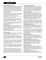
InnoSwitch3-AQ Audible Noise Reduction Engine The InnoSwitch3-AQ features an active audible noise reduction mode whereby the controller (via a “frequency skipping” mode of operation) avoids the resonant band (where the mechanical structure of the power supply is most likely to resonate − increasing noise amplitude) between 7 kHz and 12 kHz - 143 ms and 83 ms. If a secondary controller switch request occurs within this time window from the last conduction cycle, the gate drive to the power MOSFET is inhibited. Maximum Secondary Inhibit Period Secondary requests to initiate primary switching are...
Open the catalog to page 6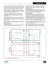
InnoSwitch3-AQ the voltage across the primary switch is near its minimum voltage when the converter operates in discontinuous conduction mode (DCM). This mode of operation is automatically engaged in DCM and disabled once the converter moves to continuous-conduction mode (CCM). Rather than detecting the magnetizing ring valley on the primaryside, the peak voltage of the FORWARD pin voltage as it rises above the output voltage level is used to gate secondary requests to initiate the switch “ON” cycle in the primary controller. FORWARD pin. In the event that the voltage on the ISENSE pin exceeds...
Open the catalog to page 7All Power Integrations catalogs and technical brochures
 InnoSwitch4-CZ
30 Pages
 LinkSwitch-TNZ
24 Pages
 2SIS0400T2C0C-33
10 Pages
 2SMS0220D2C0C-CM1200DC-34X
8 Pages
 2SML0220D2E0-FF600R17ME4
4 Pages
 2SIL1200T2A0-33
4 Pages
 InnoSwitch3-TN
23 Pages
 ChiPhy
6 Pages
Archived catalogs
 DPA-Switch
34 Pages
 CAPZero
8 Pages
 HiperPLC
26 Pages
 LinkSwitch-TN
20 Pages
 LinkSwitch-II
10 Pages
 TinySwitch-PK
24 Pages
 HiperPLC
26 Pages
 LinkSwitch-CV
20 Pages
 LinkSwitch-LP
16 Pages
 TinySwitch-III
24 Pages
 TOPSwitch-HX
48 Pages
 PeakSwitch
24 Pages
 PeakSwitch™ Family
4 Pages
- DC power supply
- AC/DC power supply
- Switched-mode power supply
- DC-DC converter
- Isolated DC-DC converter
- Transistor module
- High-voltage power supply
- SMD capacitor
- High-speed diode
- SMD DC-DC converter
- MOSFET transistor
- Step-down DC-DC converter
- DC/DC converter for telecom applications
- Printed circuit board power supply
- LED driver
- Adjustable LED driver