
Catalog excerpts

CHY100 ChiPhy™ Family Charger Interface Physical Layer IC Product Highlights • Fully supports Quick Charge 2.0 specification • Class A: 5 V, 9 V, and 12 V output voltage • Class B: 5 V, 9 V, 12 V, and 20 V output voltage USB battery charging specification revision 1.2 compatible • Automatic USB DCP shorting D+ to D- line • Default 5 V mode operation Supports TOPSwitch and TinySwitch Very low power consumption • Below 1 mW at 5 V output Fail safe operation • Adjacent pin-to-pin short-circuit fault • Open circuit pin fault Typical Applications • Battery chargers for smart phones, tablets, netbooks, digital cameras, and bluetooth accessories • USB power output ports Feedback Network Typical Application Schematic. Package Option. Description CHY100 is a low-cost USB high-voltage dedicated charging port (HVDCP) interface IC for the Quick Charge 2.0 specification. It incorporates all necessary functions to add Quick Charge 2.0 capability to Power Integrations’ switcher ICs such as TOPSwitch or TinySwitch and other solutions employing traditional feedback schemes. CHY100 supports the full output voltage range of either Class A or Class B. Optionally Class B can be inhibited for protecting the battery charger from accidental damage. CHY100 automatically detects whether a connected Powered Device (PD) is Quick Charge 2.0 capable before enabling output voltage adjustment. If a PD not compliant to Quick Charge 2.0 is detected the CHY100 disables output voltage adjustment to ensure safe operation with legacy 5 V only USB PDs.
Open the catalog to page 1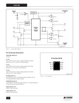
(LOOKUP TABLE) Functional Block Diagram. Pin Functional Description GROUND (GND) Pin Ground. V1 Pin Open Drain input of output voltage adjustment switch. Active for 9 V, 12 V, and 20 V output setting. V2 Pin Open Drain input of output voltage adjustment switch. Active for 12 V, and 20 V output setting. V3 Pin Open Drain input of output voltage adjustment switch. Active for 20 V output setting. BYPASS (BP) Pin Connection point for an external bypass capacitor for the internally generated supply voltage. REFERENCE (R) Pin Connected to internal band-gap reference. Provides reference current...
Open the catalog to page 2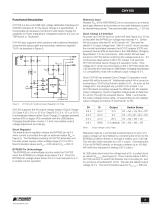
CHY100 Functional Description CHY100 is a low-cost USB high-voltage dedicated charging port (HVDCP) interface IC for the Quick Charge 2.0 specification. It incorporates all necessary functions to add Quick Charge 2.0 capability to Power Integrations’ integrated switcher ICs such as TOPSwitch or TinySwitch. CHY100 also supports other solutions with traditional feedback schemes like optocoupler and secondary reference regulator TL431 as depicted in Figure 5. VOUT D1 Reference Input Resister RREF at the REFERENCE pin is connected to an internal band gap reference and provides an accurate...
Open the catalog to page 3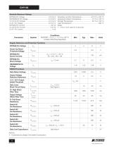
Conditions SOURCE = 0 V; TJ = -5 °C to +80 °C (Unless Otherwise Specified) Supply, Reference and Protection Functions BYPASS Pin Voltage Power-Up Reset Threshold Voltage BYPASS Pin Source Current BYPASS Pin Shunt Voltage Data Detect Voltage Output Voltage Selection Reference 12 V / 20 V Output Inhibit Threshold Data Lines Short-Circuit Delay D+ High Glitch Filter Time Output Voltage Glitch Filter Time REFERENCE Pin Voltage HVDCP Functions Data Line Capacitance NOTES: A. Guaranteed by design. Not tested in production. 4 Rev. A 07/13
Open the catalog to page 4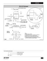
GAUGE PLANE SEATING PLANE Reference Solder Pad Dimensions Notes: 1. JEDEC reference: MS-012. 2. Package outline exclusive of mold flash and metal burr. 3. Package outline inclusive of plating thickness. 4. Datums A and B to be determined at datum plane H. 5. Controlling dimensions are in millimeters. Inch dimensions are shown in parenthesis. Angles in degrees. PI-5615-041210 Part Ordering Information • ChiPhy Product Family • 100 Series Number • Package Identifier CHY 100
Open the catalog to page 5
Initial Release. For the latest updates, visit our website: www.powerint.com Power Integrations reserves the right to make changes to its products at any time to improve reliability or manufacturability. Power Integrations does not assume any liability arising from the use of any device or circuit described herein. POWER INTEGRATIONS MAKES NO WARRANTY HEREIN AND SPECIFICALLY DISCLAIMS ALL WARRANTIES INCLUDING, WITHOUT LIMITATION, THE IMPLIED WARRANTIES OF MERCHANTABILITY, FITNESS FOR A PARTICULAR PURPOSE, AND NON-INFRINGEMENT OF THIRD PARTY RIGHTS. Patent Information The products and...
Open the catalog to page 6All Power Integrations catalogs and technical brochures
-
InnoSwitch3-AQ
28 Pages
-
InnoSwitch4-CZ
30 Pages
-
LinkSwitch-TNZ
24 Pages
-
2SIS0400T2C0C-33
10 Pages
-
2SMS0220D2C0C-CM1200DC-34X
8 Pages
-
2SML0220D2E0-FF600R17ME4
4 Pages
-
2SIL1200T2A0-33
4 Pages
-
InnoSwitch3-TN
23 Pages
Archived catalogs
-
HiperPLC
26 Pages
-
DPA-Switch
34 Pages
-
CAPZero
8 Pages
-
PeakSwitch™ Family
4 Pages
-
PeakSwitch
24 Pages
-
HiperPLC
26 Pages
-
TOPSwitch-HX
48 Pages
-
TinySwitch-PK
24 Pages
-
TinySwitch-III
24 Pages
-
LinkSwitch-TN
20 Pages
-
LinkSwitch-LP
16 Pages
-
LinkSwitch-II
10 Pages
-
LinkSwitch-CV
20 Pages


