Catalog excerpts

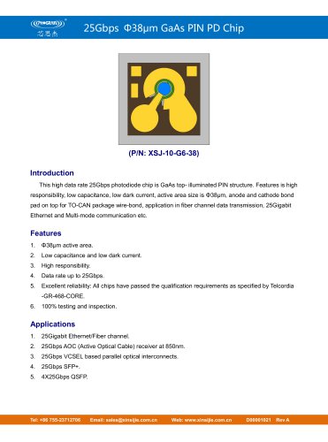
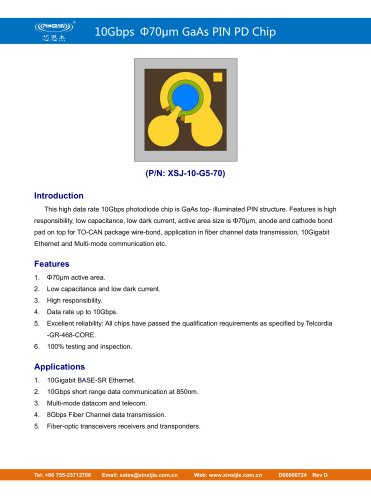
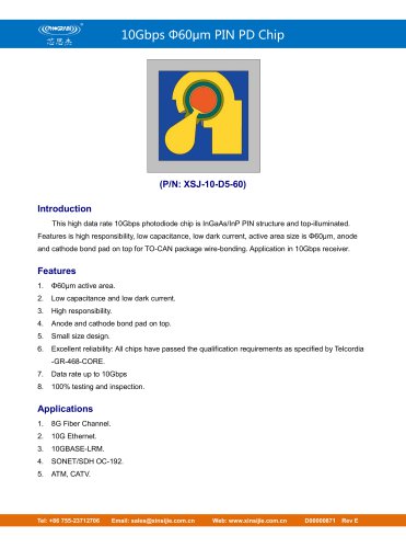
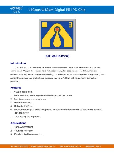
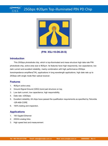
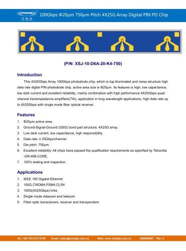
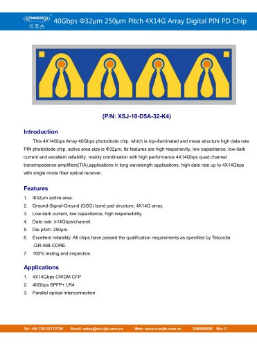
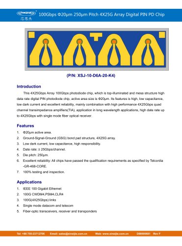
(P/N: XSJ-10-D6-20-KB) Introduction This 25Gbps photodiode chip, which is bottom-illuminated and mesa structure high data rate PIN photodiode chip, bottom active area size is Φ20μm. Its features have high responsivity, low capacitance, low dark current and excellent reliability, mainly combination with high performance 25Gbps transimpedance amplifiers(TIA), applications in long wavelength applications, high date rate up to 25Gbps with single mode fiber optical receiver. Bottom-illuminated: Φ20μm active area. Ground-Signal-Ground (GSG) bond pad structure on top. Low dark current, low capacitance, high responsibility. Bottom-illuminated type: suiting for flip-chip process. Excellent reliability: All chips have passed the qualification requirements as specified by Telcordia -GR-468-CORE. High speed test and measurement Email: sales@xinsijie.com.cn
Open the catalog to page 1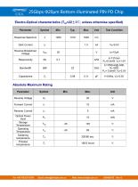
Tel: +86 755-23712706 Email: sales@xinsijie.com.cn Web: www.xinsijie.com.cn D00000753 Rev G
Open the catalog to page 2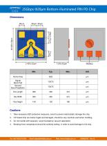
1. Take necessary ESD protective measures, avoid to prevent electrostatic damage the chip. 2. InP-based chip are easily fragile and damaged, should be very carefully used when handling. 3. Do not handle with tweezers, recommended by vacuum adsorption. 4. Bonding force, temperature should be carefully setting, in order to avoid damage to the chip. Tel: +86 755-23712706 Email: sales@xinsijie.com.cn Web: www.xinsijie.com.cn D00000753 Rev G
Open the catalog to page 3


