- Catalogs
- PHOGRAIN TECHNOLOGY(SHENZHEN) CO., LTD.
- XSJ-10-D5-45-S/10Gbps Φ45μm Digital PIN PD Chip/PHOGRAIN


- Company
- Products
- Catalogs
- News & Trends
- Exhibitions
XSJ-10-D5-45-S/10Gbps Φ45μm Digital PIN PD Chip/PHOGRAIN
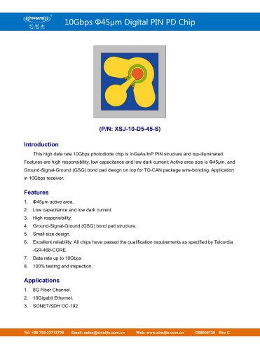
XSJ-10-D5-45-S/10Gbps Φ45μm Digital PIN PD Chip/PHOGRAIN
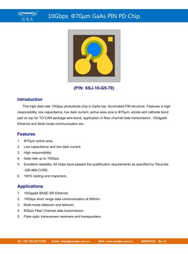
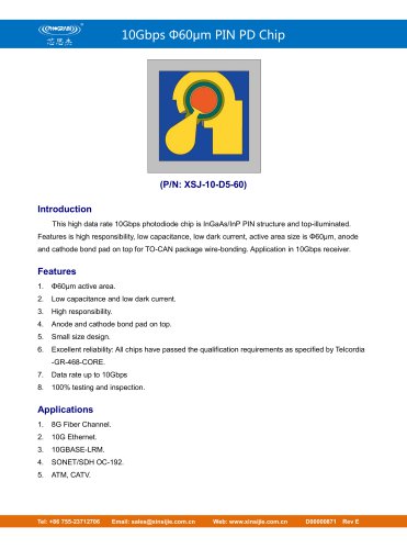
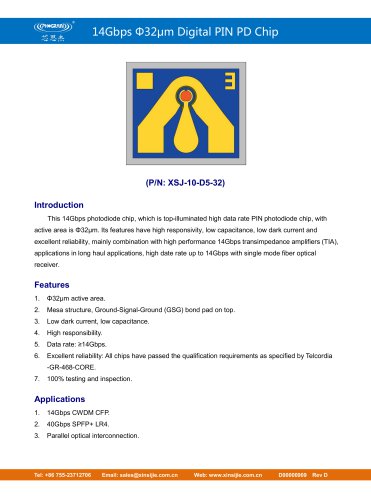
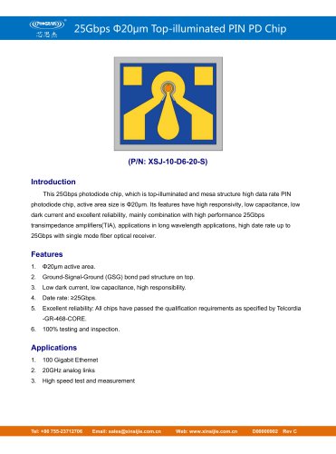
This document details a high data rate 10Gbps photodiode chip with an InGaAs/InP PIN structure, designed for top illumination. It features a 45μm active area and is suitable for 10Gbps receivers.
Features
- 45μm active area.
- Low capacitance and dark current.
- High responsivity.
- Ground-Signal-Ground (GSG) bond pad structure.
- Compact design.
- Reliability confirmed by Telcordia-GR-468-CORE standards.
- Data rate capability up to 10Gbps.
- 100% testing and inspection.
Applications
- 8G Fiber Channel.
- 10Gigabit Ethernet.
- SONET/SDH OC-192.
Electro-Optical Characteristics
Operating at 22±3℃, the chip has a response spectrum of 910-1650 nm, dark current of 0.05-0.5 nA at VR=5.0V, and a reverse breakdown voltage of 30V. Responsivity is 0.95-1.08 A/W depending on wavelength, with a bandwidth of 9.0-10.5 GHz.
Absolute Maximum Ratings
- Reverse Voltage: 20V
- Forward Current: 10mA
- Reverse Current: 5mA
- Optical Power Input: 10mW
- Storage Temperature: -45 to 125℃
- Operating Temperature: -40 to 85℃
- Storage Humidity: up to 85% r.h.
- Soldering Process Temperature: 320℃ for 60s
- Process Temperature: 150℃ for 24h
Dimensions
- Active Area: 45μm
- Signal Bond Pad: 80μm
- Ground Bond Pad: 75μm
- Die Length/Width: 240-260μm
- Die Height: 110-130μm
Cautions
- Implement ESD protective measures to prevent electrostatic damage.
- Handle InP-based chips with care due to fragility.
- Avoid using tweezers; vacuum adsorption is recommended.
- Carefully set bonding force and temperature to avoid chip damage.
Catalog excerpts

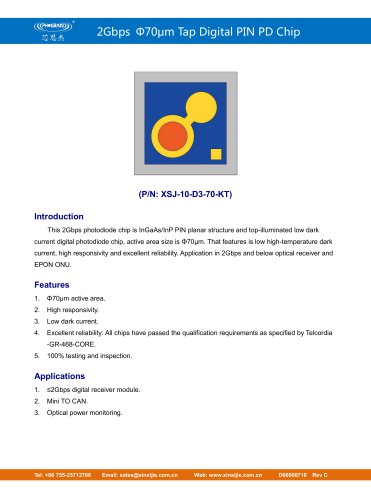
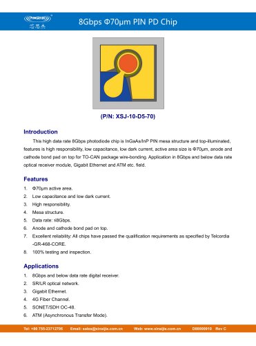
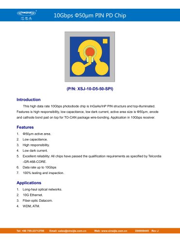
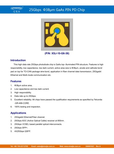
(P/N: XSJ-10-D5-45-S) Introduction This high data rate 10Gbps photodiode chip is InGaAs/InP PIN structure and top-illuminated. Features are high responsibility, low capacitance and low dark current; Active area size is Φ45μm, and Ground-Signal-Ground (GSG) bond pad design on top for TO-CAN package wire-bonding. Application in 10Gbps receiver. Low capacitance and low dark current. High responsibility. Ground-Signal-Ground (GSG) bond pad structure. Small size design. Excellent reliability: All chips have passed the qualification requirements as specified by Telcordia -GR-468-CORE. Email: [email protected]
Open the catalog to page 1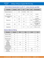
Tel: +86 755-23712706 Email: [email protected] Web: www.xinsijie.com.cn D00000720 Rev C
Open the catalog to page 2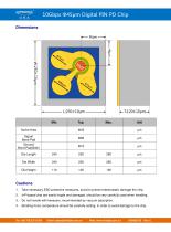
1. Take necessary ESD protective measures, avoid to prevent electrostatic damage the chip. 2. InP-based chip are easily fragile and damaged, should be very carefully used when handling. 3. Do not handle with tweezers, recommended by vacuum adsorption. 4. Bonding force, temperature should be carefully setting, in order to avoid damage to the chip. Tel: +86 755-23712706 Email: [email protected] Web: www.xinsijie.com.cn D00000720 Rev C
Open the catalog to page 3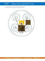
Recommended for chip’s die bonding and wire bond: Email: [email protected]
Open the catalog to page 4All PHOGRAIN TECHNOLOGY(SHENZHEN) CO., LTD. catalogs and technical brochures
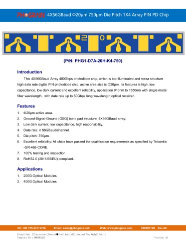 PHG1-D7A-20H-K4-750
3 Pages
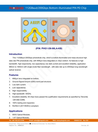 PHG1-D8-90LA-KB
4 Pages