- Catalogs
- Park Systems
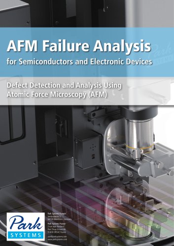
- AFM Failure Analysis for Semiconductors and Electronic Devices
- Company
- Products
- Catalogs
- News & Trends
- Exhibitions
AFM Failure Analysis for Semiconductors and Electronic Devices
1 /12Pages
AFM Failure Analysis for Semiconductors and Electronic Devices
1 /12Pages
Catalog excerpts

AFM Failure Analysis for Semiconductors and Electronic Devices Defect Detection and Analysis Using Atomic Force Microscopy (AFM) Park Systems Europe Janderstrasse 5 68199 Mannheim, Germany Park Systems France 2 rue Jean Rostand Parc Orsay Université 91400 ORSAY, France [email protected] www.parksystems.com
Open the catalog to page 1
• SSRM AFM - High Vacuum Scanning Spreading Resistance Microscopy • C-AFM - Conductive Atomic Force Microscopy • SCM - Scanning Capacitance Microscopy SSRM AFM for Optimal Results in Semiconductor Failure Analysis The High Vacuum Scanning Spreading Resistance Microscopy (SSRM), available on Park NX-Hivac, enables 2D carrier profiling of next generation devices and measures the high resolution SSRM image under high vacuum conditions to improve production yield. The high vacuum SSRM measurements show much higher accuracy and resolution than in ambient conditions. Thanks to the very high sensitivity...
Open the catalog to page 2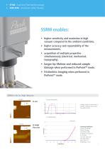
• SThM - Scanning Thermal Microscopy • ADR AFM - Automatic Defect Review SSRM enables: • higher sensitivity and resolution in high vacuum compared to the ambient conditions, • higher accuracy and repeatability of the measurements, • acquisition of multiple properties simultaneously (electrical, mechanical, topography), • longer tip lifetime and reduced sample damage when performed in PinPointTM mode, • frictionless imaging when performed in PinPointTM mode. SSRM in Air vs. High Vacuum µm Current line profile Stronger current in vacuum than in ambient conditions due to better tip-sample contact....
Open the catalog to page 3
• SSRM AFM - High Vacuum Scanning Spreading Resistance Microscopy • C-AFM - Conductive Atomic Force Microscopy • SCM - Scanning Capacitance Microscopy Conductive AFM as AFM Failure Analysis for Electrical Devices Conductive AFM (C-AFM) simultaneously measures topography and electrical properties (conductivity) of samples by using the AFM tip as a nanometer-scale electrical probe. More specifically, it monitors the current flow between the conductive tip and sample, and when the bias is applied. At the same time, it records the cantilever deflection as the tip scans over the sample surface. The...
Open the catalog to page 4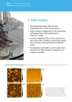
• SThM - Scanning Thermal Microscopy • ADR AFM - Automatic Defect Review C-AFM enables: • obtaining high quality data for both topography and current measurements, • high resolution imaging due to the elimination of frictional force when performed in PinPointTM mode, • accurate mapping of the current variations at the surface due to ability to control the contact force and time when performed in PinPointTM mode, • homogeneous and higher current signal when performed in High Vacuum in comparison to ambient condition. C-AFM in Air vs. High Vacuum 2 nm high vacuum High Vacuum C-AFM from the same...
Open the catalog to page 5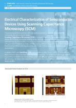
• SSRM AFM - High Vacuum Scanning Spreading Resistance Microscopy • C-AFM - Conductive Atomic Force Microscopy • SCM - Scanning Capacitance Microscopy Electrical Characterization of Semiconductor Devices Using Scanning Capacitance Microscopy (SCM) Characterizing electrical properties with high spatial resolution is a key in understanding the functionality of a semiconductor device. Scanning Capacitance Microscopy (SCM) is a powerful method to characterize semiconductor devices due to its non-destructive scanning ability, and high accuracy in measurements with nanoscale features. SCM enables simultaneously...
Open the catalog to page 6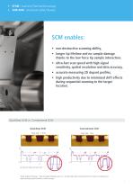
• SThM - Scanning Thermal Microscopy • ADR AFM - Automatic Defect Review SCM enables: • non-destructive scanning ability, • longer tip lifetime and no sample damage thanks to the low force tip sample interaction, • ultra-fast scan speed with high signal sensitivity, spatial resolution and data accuracy, • accurate measuring 2D dopant profiles, • high productivity due to minimized drift effects during sequential zooming to the target location. QuickStep SCM vs. Conventional SCM QuickStep SCM Higher Quality SCM Image - High Throughput QuickStep Scan is 5~10 times faster than conventional SCM scan...
Open the catalog to page 7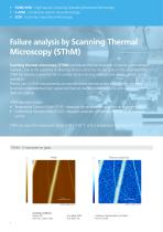
• SSRM AFM - High Vacuum Scanning Spreading Resistance Microscopy • C-AFM - Conductive Atomic Force Microscopy • SCM - Scanning Capacitance Microscopy Failure analysis by Scanning Thermal Microscopy (SThM) Scanning thermal microscopy (SThM) investigates thermal properties of various nanostructured materials. Due to the capability of detecting failures caused by the hot spots on the sample surface, SThM has become a powerful tool to analyze semiconducting materials and devices at high spatial resolution. The key part of SThM measurements are nanofabricated thermal probes with resistive elements...
Open the catalog to page 8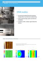
• SThM - Scanning Thermal Microscopy • ADR AFM - Automatic Defect Review SThM enables: • measuring localized thermal properties (temperature, local thermal conductivity), • unprecedented high spatial and thermal resolution, • sensitivity with a unique signal detection scheme. SThM - Pole-Tip-Recession of HDD Head nm Power was applied to (A) and (B) region on height. Simultaneously the thermal images were obtained by Temperature Constant Mode (TCM), SThM. Temperature distribution was obtained. SThM Image SThM Image SThM Image
Open the catalog to page 9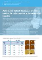
• SSRM AFM - High Vacuum Scanning Spreading Resistance Microscopy • C-AFM - Conductive Atomic Force Microscopy • SCM - Scanning Capacitance Microscopy Automatic Defect Review as an inline method for defect review in Semiconductor Industry Addressing the continuously decreasing size of semiconductor devices in modern technology, AFM provides a high-resolution and non-destructive analysis method for defect review at the semiconductor industry. The Automatic Defect Review (ADR) AFM, introduced by Park Systems, is an automated process, which simplifies and speeds up the previously time-consuming...
Open the catalog to page 10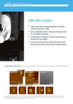
• SThM - Scanning Thermal Microscopy • ADR AFM - Automatic Defect Review ADR AFM enables: • simple and time-saving workflow for defect characterization in AFM, • fully automated defect characterization of four to ten defects per hour, • visualization of defects in three dimensions at nanometer-resolution, • non-destructive surface characterization and low tip wear due to non-contact measurement. ADR SEM scan area ADR SEM scan area 10 µm c) ADR AFM of electron beam damage Comparison between ADR AFM and ADR SEM, a) AFM image of bump defect missed previously by ADR SEM. The ADR SEM scan area is...
Open the catalog to page 11All Park Systems catalogs and technical brochures
 Research Product Overview
2 Pages
 Products Overview
15 Pages
- Microscope
- Laboratory microscope
- Inspection microscope
- Measuring microscope
- Automated microscope
- High-resolution microscope
- Industrial microscope
- Research microscope
- Modular microscope
- Motorized microscope
- Near field probe microscope
- CCD microscope
- Atomic force microscope
- Metrology microscope
- Scanning probe microscope
- Microscope for the chemical industry
- Super-resolution microscope
- Big sample microscope