
- Catalogs
- PALOMAR TECHNOLOGIES
- Palomar Microelectronics

Palomar Microelectronics

Palomar Microelectronics
Palomar Microelectronics provides a range of services including package design and analysis, prototyping, pilot builds, SMT, wire bonding, component placement, metrology services, ball bumping, and package sealing. These services leverage years of packaging experience to develop and validate processes before production equipment investment.
The company works with various devices such as RF amplifiers, flip chips, MEMS/MOEMS, LEDs, solar devices, stacked die, direct chip attach, optical devices, hybrids, implantable devices, stud bumping, thermosonic attach, and high-bright LEDs.
- Cost-effective alternative to capital equipment investment.
- Immediate access to manufacturing expertise and increased capacity.
- Quick and efficient evaluation of prototype devices and manufacturing methods.
- Reduced time to market and increased yield with volume production solutions.
Palomar offers in-house process development or a research and development partnership. A private lab is available for engineering teams with comprehensive process support.
- Wire Bonding: Gold or aluminum wire, round wire or ribbon, and stud bumping with fine pitch, deep access, and large work areas.
- Die Attach: Epoxy, eutectic, thermosonic, and thermocompression attachments with deep access and large work areas.
- Test & Metrology: Full metrology services including SEM, elemental analysis, SAM, and various testing systems.
- Palomar Technology Partnerships: Component handling, wafer saw, surface mount, package sealing, and failure analysis services.
- Component Assembly Work Cell: Automated assembly, laser diode attach, precision eutectic die bonder, RF component assembly, LED gang reflow.
- Wire Bonding: Deep access wedge bonders, chain stitch bonding, gold stud bumping, precision ball & stitch bonders.
- Packaging: Volumetric nanoliter dispense, plasma cleaning system, pulsed heat reflow, vacuum bake-out, plasma pen.
- Metrology: Scanning electron microscope, optical inspection microscope, scanning acoustic microscope, wire pull and shear test system.
- Information Collection: Submit a detailed scope of the development project.
- Evaluation: Discuss application and project requirements.
- Quotations: Receive a detailed quote including process requirements and pricing.
- Process Development: Delivery typically within one month of order placement.
- Communication: Regular status reports provided.
- Deliverables: Pilot runs, detailed reports, test data, and low volume manufacturing support.
Catalog excerpts
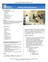
Services Offered: Package Design and Analysis Prototyping Pilot Builds SMT Wire Bonding Component Placement Metrology Services Ball Bumping Package Sealing Benefits: We apply ideas and solutions from years of packaging experience so that Palomar Technologies can develop and validate your process before you invest in production equipment. Typical Devices: RF Amplifiers Flip Chip MEMS / MOEMS LEDs Solar Application Categories: Stacked Die Direct Chip Attach 1. Wire Bonding Gold or aluminum wire, round wire or ribbon, and stud bumping needs. Fine pitch, deep access, and large work areas available. 2. Die Attach ח Epoxy, eutectic, thermosonic, and thermocompression attachments. Deep access, large work areas, steady-state, and pulsed heat control. Accuracies up to 1.5 micron, 3 sigma. 3. Test & Metrology Full metrology services including SEM, elemental analysis, SAM, XYZ optical microscopes, wire pull and shear tester, die shear tester.4. Palomar Technology ז partnerships: a. Component handling b. Wafer saw c. Surface mount d. Package sealing e. Failure analysis services i. X-section ii. Elemental analysis iii. X-Ray Microscope Optical Devices Hybrids Implantable Devices Stud Bumping Thermosonic Attach High Bright LEDs Why choose Palomar Microelectronics process development & prototyping services? Achieve a cost-effective alternative to investing in capital equipment. Gain immediate access to manufacturing expertise and increased capacity without making staff increases. Evaluate prototype devices and manufacturing methods quickly and efficiently. Reduce time to market. Increase yield with a volume production solution. Options: Our applications engineers can develop your process in-house, or we can form a research and development partnership with your company. A separate private lab is available to accommodate an engineering team from your company with as much process support as you may require from our Applications team. A comprehensive range of services are offered out of our private lab in Carlsbad. Palomar Technologies Inc. 2728 Loker Avenue West Carlsbad, CA 92010 Phone 760.931.3600 Fax 760.931.5191 >
Open the catalog to page 1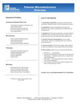
Component Assembly Work Cell: 1. Information Collection: Customer submits a form providing a detailed scope of their development project. Automated Component Assembly Cell Laser Diode Attach Precision Eutectic Die Bonder RF Component Assembly Cell LED Gang Reflow 2. Evaluation: Palomar Engineers discusses the application and project requirements to determine the overall scope. 3 . Quotations: Palomars applications manager defines a detailed quote including each process required, the piece part price plus the estimated total project price. Wire Bonding Deep Access Wedge Bonders Chain Stitch Bonding...
Open the catalog to page 2All PALOMAR TECHNOLOGIES catalogs and technical brochures


Archived catalogs
 Model 3470-II Wedge Bonder
2 Pages
 Model 2470-V Wedge Bonder
2 Pages


- Kiln
- Chamber kiln
- Heat treatment kiln
- Sorting machine
- Combustion kiln
- Gas kiln
- Controlled atmosphere oven
- Automatic sorting system
- Vacuum oven
- Manual cleaning system
- Continuous oven
- Optical sorting system
- Soldering machine
- Medical cleaning system
- Automatic soldering machine
- Brazing oven
- Interferometer
- Printed circuit soldering oven
- Automated die bonder