Group: SIEMENS

Catalog excerpts
AS1170Datasheet Published by ams-OSRAM AG Tobelbader Strasse 30, 8141 Premstaetten, Austria Phone +43 3136 500-0 ams-osram.com © All rights reserved
Open the catalog to page 1
Datasheet • PUBLIC • Document Feedback DS001083 • v1-00 • 2023-Oct-04
Open the catalog to page 2
Datasheet • PUBLIC • Document Feedback DS001083 • v1-00 • 2023-Oct-04
Open the catalog to page 3
AS1170 High current LED/VCSEL driver 1 General description The AS1170 is an inductive high efficient DCDC step up converter with two current sinks. The DCDC step up converter operates at a fixed frequency of 4 MHz and includes soft startup to allow easy integration into noise sensitive RF systems. The AS1170 includes flash timeout, overvoltage, over temperature, undervoltage and short circuit protection functions. The AS1170 is controlled by an I²C interface and has a hardware automatic shutdown if SCL=0 for 100 ms. Therefore no additional enable input is required for shutting down of the...
Open the catalog to page 4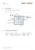
1.3 Block diagram The functional block of this device is shown below: Figure 1: Functional block of AS1170 Lccdc 1 .OjjH 2 Ordering informationProduct code Q-Number Package Delivery form Delivery quantity AS1170 Q65113A7128 AS1170 WLP LF T&R Tape and reel 10000 pcs Datasheet • PUBLIC • Document Feedback DS001083 • v1-00 • 2023-Oct-04
Open the catalog to page 5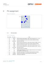
amin osram 3 Pin assignment Figure 2: Pin assignment 3.1.1 Pin description Table 2: Pin description Pin number Pin name Datasheet • PUBLIC • Document Feedback DS001083 • v1-00 • 2023-Oct-04 DCDC converter output capacitor - make a short connection to Cvout / Vout2. Power and analog ground; make a short connection between both balls. Flash LED current sink. DCDC converter switching node - make a short connection to SW2 / coil Ldcdc. Power and analog ground; make a short connection between both balls. DCDC converter output capacitor - make a short connection to Cvout / Vouti DCDC converter...
Open the catalog to page 6
AS1170 Absolute maximum ratings amin osram 4 Absolute maximum ratings Stresses beyond those listed under "Absolute Maximum Ratings” may cause permanent damage to the device. These are stress ratings only. Functional operation of the device at these or any other conditions beyond those indicated under "Operating Conditions” is not implied. Exposure to absolute maximum rating conditions for extended periods may affect device reliability. Table 3: Absolute maximum ratings of AS1170 Parameter Min Max Unit Comments Note: Diode between VOUT1/2 and SW1/2 Voltage between GND pins Input pin current...
Open the catalog to page 7
Moisture sensitivity level (MSL) Comments Represents a max. floor life time of unlimited (1) Depending on actual PCB layout and PCB used measured on demoboard; for peak power dissipation during flashing see document AS1170 thermal measurements. (2) PDERATE de-rating factor changes the total continuous power dissipation (PT) if the ambient temperature is not 70 °C. Therefore for e.g. TAMB = 85 °C, calculate PT at 85 °C = PT - PDERATE * (85 °C to 70 °C). (3) Pins LED_OUT1 connected to LED_OUT2 and capacitor CVOUT connected to VOUT1/2 and GND; both GND pins connected together. (4) Measured on...
Open the catalog to page 8
Datasheet • PUBLIC • Document Feedback DS001083 • v1-00 • 2023-Oct-04
Open the catalog to page 9
amin osram Symbol Parameter Condition Min Typ. Max Unit Vledshort Flash LED short circuit detection voltage Overtemperature protection Overtemperature hysteresis Voltage measured between pins VOUT 1,2 and LED_OUT1,2 Junction temperature Flash timeout timer Undervoltage lockout Can be adjusted with register flash_timeout Accuracy Falling Vvin Rising Vvin Vuvlo+ Vuvlo+ Vuvlo+ High level input voltage Low level input voltage High level input voltage Low level input voltage Low level output voltage Leakage current Pins SCL, SDA Pins STROBE In indicator, assist or flash mode, if SCL is low...
Open the catalog to page 10
I²C specifications Table 5: I²C specifications Symbol I²C mode timings – see Figure 3 fSCLK Bus free time between a STOP and START condition Hold time (repeated) START Condition(7) HIGH period of SCL clock Setup time for a repeated START condition Rise time of both SDA and SCL signals Fall time of both SDA and SCL signals Setup time for STOP condition Capacitive load for each bus line 0.6 CB - total capacitance of one bus line in pF (1) For VBAT=4.5 V, SCL=1.8 V, SDA=1.8 V maximum ISTANBY is <16 µA. (2) To improve efficiency at low output currents, the active part of the internal switching...
Open the catalog to page 11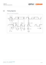
Timing diagrams Figure 3: I²C mode timing diagram Datasheet • PUBLIC • Document Feedback DS001083 • v1-00 • 2023-Oct-04
Open the catalog to page 12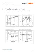
AS1170 Typical operating characteristics Typical operating characteristics VVIN = 3.7 V, TA = 25 °C (unless otherwise specified), LED: ams OSRAM Phaser 2 (VFLED = 3.8 V at 1 A). Figure 4: DCDC efficiency vs. VVIN Figure 5: Application efficiency (PLED/PVIN) vs. VVIN Figure 6: Battery current vs. VVIN Figure 7: Efficiency at low currents (300 mA) 100 95 Datasheet • PUBLIC • Document Feedback DS001083 • v1-00 • 2023-Oct-04
Open the catalog to page 13
AS1170 Typical operating characteristics Figure 8: ILED STARTUP (ILED_OUT = 1.0 A) Figure 9: IVIN, ILED STARTUP (ILED_OUT = 800 mA) Figure 10: ILED STARTUP (ILED_OUT = 60 mA) Figure 11: VOUT / ILED_OUT ripple, ILED_OUT = 1.0 A Datasheet • PUBLIC • Document Feedback DS001083 • v1-00 • 2023-Oct-04
Open the catalog to page 14
AS1170 Typical operating characteristics Figure 12: ILED rampdown (ILED_OUT = 1.0 A) Figure 13: ILED_OUT vs. TAMB 63 Figure 14: Oscillator frequency fCLK vs. TAMB Figure 15: Flash timeout Datasheet • PUBLIC • Document Feedback DS001083 • v1-00 • 2023-Oct-04
Open the catalog to page 15
Detailed description The AS1170 is a high performance DCDC step up converter with internal PMOS and NMOS switches. Its output is connected to one or two flash LEDs1 with an internal current sink. The device is controlled by the pins SDA and SCL in I²C mode. The actual operating mode like standby, assist light, indicator or flash mode, can then be chosen by the interface. If not in standby mode, the device automatically enters shutdown mode by keeping SCL low for more than t2. The AS1170 includes a fixed frequency DCDC step-up with accurate startup control. Together with the current sink (on...
Open the catalog to page 16All OSRAM Opto Semiconductors catalogs and technical brochures
-
 SFH 4775S
21 Pages
-
 LG Q976.01
24 Pages
-
 LE BR Q7WM.0A
28 Pages
-
 GW CSSRM4.HW
23 Pages
-
 SFH 4851
15 Pages
-
 SFH 464
14 Pages
-
 SFH 4725AS A01
20 Pages
-
 SFH 4726AS
19 Pages
-
 PLPT9 450LB_E A01
16 Pages
-
 LOG T77K
16 Pages
-
 SFH 4855
13 Pages
-
 KRTB EKLP42.32
27 Pages
-
 LRTBGRTG
26 Pages
-
 LB QH9G
22 Pages
-
 KR EGLP41.22
19 Pages
-
 Laser Diodes
8 Pages
-
 LED for General Lighting (SSL)
22 Pages
-
 Infrared Components
62 Pages
-
 Blue Laser
9 Pages
-
 Proximity Sensor SFH 7741
7 Pages
-
 Tape and Reel
34 Pages
-
 Intelligent Displays
22 Pages
-
 Light Emitting Diodes (LED)
74 Pages
-
 Schmitt-Trigger Brochure
4 Pages
-
 Enstackable clips
6 Pages
-
 Golden Dragon Plus
2 Pages
-
 High Power lasers
14 Pages


