Wafer and PCB control with Opto's 'Machine Vision Microscopes' (4 pages)
1 /4Pages

Wafer and PCB control with Opto's 'Machine Vision Microscopes' (4 pages)
1 /4Pages
Catalog excerpts
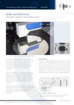
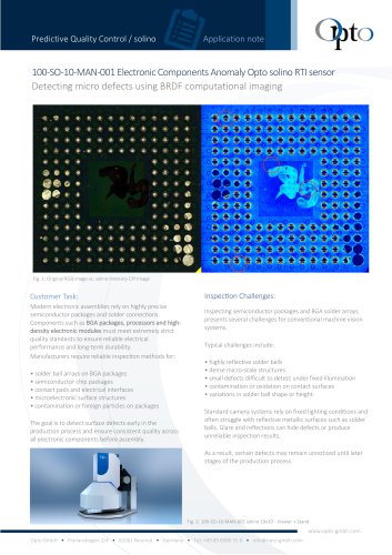
Test & Measurement / Semicon Electronics Wafer and PCB Control with Opto’s ‘Machine Vision Microscopes’ Fig. 1: Imaging Module compact M IC10-05o33MU3101 with 37mm WD . Electronics are an essential part in nearly every device we are using daily. The demand is high, the volumes huge, the size miniaturized, the price normally quite low, but the high throughput inspection needs throughout all the production steps are extremely high and must be fully automated. The optical inspection is – besides the electrical testing – one of the most important technologies in all Quality Control levels. As the Opto Imaging Modules are pure plug & play digital microscopes, they are by nature done for integration into AOI machines and for the need of digital manual inspection. PCB Inspection The new Opto Imaging Modules could be easily integrated in every machine or workstation for accurate printed circuit board (PCB) quality control, rework, failure analysis or documentation process. The time for optical microscopes is over, the operator wants to work purely on a screen and the Quality department wants Industry 4.0 compliance. The new machine vision microscopes have a LED coax- and ring light integrated. Here some more detailed explanation of how our machine vision microscopes (Opto Imaging Modules with microscopic magnification higher than 1x) could assist in optimizing the optical defect screening. Fig. 2: Coaxial LED serves as incident light bright field illumination, the integrated ring light as incident light dark field illumination www.opto-gmbh.com Opto GmbH • Floriansbogen 2/4 • 82061 Neuried • Germany • Tel: +49 89 8980 55 0
Open the catalog to page 1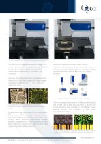
Fig. 3: IM · compact M with coaxial (left) & ring light illumination (right) The IM•linea M Imaging Module with a bigger FoV , or the machine vision microscope compact M could be considered as pure digital microscopes for single-sided, double-sided, or multilayer PCB inspection. Besides this typical microscope tasks, and also automated measurements like pin counts, pin distance control, components identification or identifying wrong polarity assemblies could be done with the Imaging Modules. Normally the components to be inspected are LED diodes, IC`s, FPGA Chips, capacitors, plastic leaded chip...
Open the catalog to page 2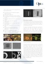
“Time is money”, that’s why the Imaging Modules allow cost-effective QC: • All modules are more compact than regular digital microscopes • Optimized for mobile use • An image in 2 Minutes on a mobile computer • Pre calibrated so immediate measurements are possible • Fatigueless inspection for one or more users on monitor • Highest image quality with huge color repeatability • Less expensive than microscopes with similar optical quality • Robust with integrated LED`s and no moving parts • Perfect mix between working distance, magnification, and size to perform best ergonomics • One unit, all embedded,...
Open the catalog to page 3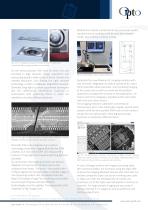
Module by module is produced to the same high quality standard and as nothing could be optically changed inside, also nothing could go wrong. Fig. 12: For imaging transparent samples like photomasks also transmitted light imaging modules are available As the semiconductor AOI must be done fast and normally in high volumes, image acquisition and processing speed is often a critical factor. Besides the needed resolution, also finding the right contrast technology is often a challenge. Brightfield (coaxial), Darkfield (ring-light) or more specialized techniques like DIC (Differential Interference...
Open the catalog to page 4All OPTO catalogs and technical brochures
 IM•profile M
2 Pages
 Machine Vision Objectives
24 Pages
 Microscope Accessories
28 Pages
 043-112414-C02
2 Pages
 100-CO24-TC
2 Pages
 CylinderInspector 2D
2 Pages
 Focus Drive C, Coarse
2 Pages
 043-603020
2 Pages
 043-112108
2 Pages
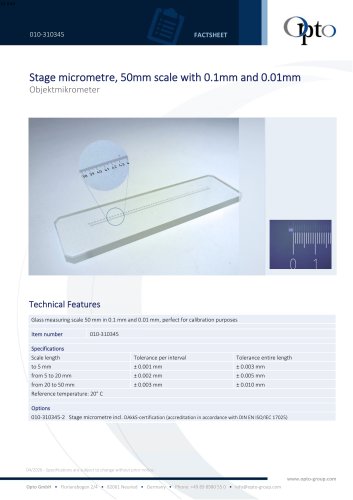 010-310345
1 Page
 100-GS100-02
2 Pages
 100-GS100-01
2 Pages
 Opto Test & Measurement
4 Pages
 Opto Medical & Life Science
4 Pages
 043-21300X
2 Pages
 IP10-06q33CU5101 four pages
4 Pages
 Opto Software
6 Pages
 Imaging Modules
6 Pages
 Trackstand
2 Pages
 043-112414-C01
2 Pages
 100-MS50-GAN
2 Pages
 100-MS50-AN
2 Pages
 100-MS25-GAN
2 Pages
 100-MS25-AN
2 Pages
 045-100130-01
2 Pages
 MMM 4.0
2 Pages
 IC10-05033CU3101 four pages
4 Pages
 IM•linea M
2 Pages
 IM•compact_M
2 Pages
 043-610022
2 Pages
 043-600505
2 Pages
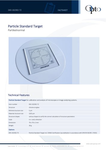 043-1022302-72
2 Pages
 Jointed Coupler
1 Page
 Tilting Table
4 Pages
 Oblique Viewing Module
4 Pages
 Jointed Couplers
4 Pages
 IM MACHINEVISIONMICROSCOPE
6 Pages


- Digital imager
- Visible imager
- CMOS camera module
- Industrial camera module
- Positioning table
- Monitoring camera system
- Full-color camera system
- Calibration system
- Translation stage
- USB camera module
- Detection camera system
- Image processing camera module
- Monochrome camera module
- GigE Vision camera
- Compact imager
- Inspection system
- Precision positioning table
- Inspection imager