- Catalogs
- Onto Innovation Inc.
- Use of Wafer Backside Inspection and SPR to Address Systemic Tool and Process Issues
Use of Wafer Backside Inspection and SPR to Address Systemic Tool and Process Issues
1 /6Pages

Use of Wafer Backside Inspection and SPR to Address Systemic Tool and Process Issues
1 /6Pages
Catalog excerpts
Use of Wafer Backside Inspection and SPR to Address Systemic Tool and Process Issues Alan Carlson, Prasad Bachiraju Rudolph Technologies, Inc. Jennifer Clark, Dale Trost IBM Corporation, Systems & Technology Group Presented at SPIE - February 2010 Defects on the backside of wafers can be either tool or process induced and can cause lithography-related issues such as focus deviation or chuck contamination. Tool induced scratches, process induced contamination, or residues on the back of wafers often have unique signatures, such as a repeatable scratch caused by wafer handling equipment or a chuck imprint on the backside of a wafer. Certain backside defect signatures such as large scratches or divots can contribute to wafer breakage or reliability issues. Detection of front surface defects on wafers has traditionally been of primary concern to semiconductor device manufacturers, while backside defects have received much less attention. Device manufacturers have now learned that backside defects can also contribute to wafer breakage, yield loss, and reliability issues. Additionally, as design rules continue to shrink with each new technology node, depth of focus decreases, making the photolithography process more sensitive to backside defects. Spatial Pattern Recognition (SPR) is a method of comparing defect patterns at the wafer level with known defect signatures stored in a library that is created from process data. These defect signatures can represent systemic issues with process tools, handling equipment, or the process itself. This paper describes a backside inspection method for identifying wafers with both known and new spatial pattern signatures. By reporting the frequency of each signature category, process partitioning can efficiently trace the source of these problems. In addition, new defect signatures can be automatically learned and added to the library. The paper also includes examples of how this method was used to identify backside defect patterns caused by process and tool excursions in a 300mm fabricator. Mechanical damage such as scratches and particles on the backsides of wafers can be caused by wafer handling equipment, such as robots, wafer chucks and lift pins, as well as by processes such as CMP. Certain types of mechanical damage such as chuck marks or deep scratches can lead to chip weakness or breakage. Often, these types of defects have characteristic patterns which can be discerned when manually viewing wafer maps. When a process tool has a mechanical issue, it can leave a unique fingerprint on the backsides of wafers, which can aid root cause analysis. Backside defect counts alone do not give a complete picture of the types of defects located on the backsides of wafers. There can be a great deal of variability in defect counts due to the amount of particles, scratches, or large patterns. This variability prevents both the proper trending of killer defects and the filtering out of nuisance defects. One solution is to manually view individual wafer maps or stack maps in order to quantify the types and frequency of defect patterns occurring on the backsides of wafers, but in a highvolume manufacturing environment, this is timeconsuming, labor-intensive, and costly.
Open the catalog to page 1
This paper describes an automated surveillance method using SPR to monitor incoming wafer inspection data for known defect signatures, and report the frequency and category of each type of signature. This method allows for a near-real time method to monitor process and tool-related excursions, classify defects, determine root causes, and take corrective action, while reducing the amount of human interaction required. Wafer Backside Inspection The data presented here was collected using an AXi™ Series frontside inspection system with integrated backside (B20™) and edge (E25™) inspection. The B20...
Open the catalog to page 2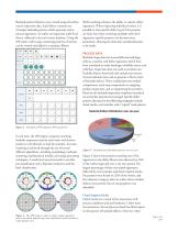
Backside pattern libraries were created using all-surface macro inspection data. Each library contains sets of unique backside patterns which represent tool or process signatures. As wafers are inspected, wafer-level data is collected in the tool-centric database. Using the SPR client, wafer maps containing patterns of interest can be viewed and added to a signature library. Wafer stacking enhances the ability to capture defect signatures. When inspecting individual wafers, it is possible to miss specific defect types if the patterns are faint, but when overlaying multiple wafer-level signatures,...
Open the catalog to page 3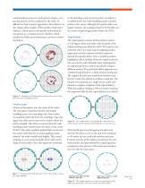
contamination occurs on a tool’s process chuck, a very specific pattern can be transferred to the wafer. In addition to their cosmetic appearance, these defects can also impact chip strength. When product inspections indicate a chuck pattern, the specific wafers must be traced back to a common process chamber, which would most likely need maintenance activity to resolve the defects. to the metrology tool, corrective action was taken to re-calibrate how the wafer handling system returned wafers to the carrier. Although this specific defect was largely cosmetic, the scraping caused by the handler...
Open the catalog to page 4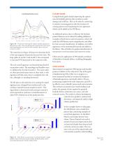
FUTURE WORK Going forward, goals include improving the capture rates for backside patterns that correlate to wafer damage and yield loss. This can be done by continuing to monitor incoming process data for instances of existing patterns and monitoring for new signatures which can be added to the SPR library. Figure 10 - Trend chart showing the relative number of patterns detected over time. Note the downward trends for the oval scratch and tripod patterns over the last three months, after corrective action was taken. The trend chart in Figure 10 shows the detection levels of the top categories...
Open the catalog to page 5
The authors would like to thank Jeff Hall, Daniel Tong, and Jeff Zia for their help in the collection and processing of data and Aaron Shepherd and Virginia Becker for their help in the preparation of this paper. REFERENCES Carlson, Alan and Le, Tuan, Rudolph Technologies, Inc., “Correlation of backside defects to hot spots using advanced macro inspection” - SPIE 6152-133. Hallen, Joseph, National Semiconductor; Carlson, Alan, Le, Tuan, Rudolph Technologies, Inc., “Improving wafer yields with integrated all-surface inspection”, - Solid State Technology, June 2007, pp 43-48. Drozda-Freeman, Andrew,...
Open the catalog to page 6All Onto Innovation Inc. catalogs and technical brochures
 Onto Innovation
19 Pages
 Solid State Technology
6 Pages
 Use style: paper title
6 Pages
 rudolph technologies
1 Page


- Management software solution
- Analysis software solution
- Process software
- Windows software
- Real-time software
- Computer-aided design software
- Design software solution
- Monitoring software solution
- Industrial software
- Visualization software solution
- Automatic tester
- Automated software
- Industrial tester
- Thickness gauge
- Development software
- Reporting software
- Machine software
- Optimization software
- Automatic inspection system