- Catalogs
- Onto Innovation Inc.
- Use style: paper title
Use style: paper title
1 /6Pages

Use style: paper title
1 /6Pages
Catalog excerpts
Through Silicon Via Process Characterization by Integrated Inspection/Metrology Solutions in Visible and Infrared Domain Category: AM: Advanced Metrology Nicolas Devanciard, Stephane Rey, Thomas Magis, Stephane Minoret, Carlos Beitia CEA, LETI, Minatec campus Grenoble, France [email protected] Abstract - In this paper, we present an integrated in-line solution, combining automatic visual inspection/classification with unique 2D/3D measurement technologies, which was used to characterize the detectivity and the morphology of open through silicon via (TSV) structures. The measurements were performed on 300mm Si wafers hosting several populations of via with diameter varied from 5 to 20 micron, and target aspect ratio from 1:8 to 1:20. Interferometry techniques coupled with high resolution cameras working in white light and infrared domains were used to demonstrate TSV process control in R&D and high volume manufacturing environments. Topics - Advanced Metrology, Defectivity, Process Control, 3D/TSV/Interpose, Interferometry I. Introduction The 3D/TSV approach is an emerging technology which is steadily gaining momentum. Recent advances in thin wafer processing and chip stacking have demonstrated High Volume Manufacturing capability [1]. However, some critical processing steps still need to be optimized. Current concerns include the presence of particles inside the open via, process uniformity over the wafer, and aspect ratio. Therefore, improving the process development by reducing development time is of paramount importance. Several techniques have been proposed in the recent past to characterize TSV processes in line. For example, interferometry [2] and reflectometry [3] have already proved the metrology capability to estimate the via depth, but the lack of defective control on the wafer investigated did not allow certitude of outgoing results, preventing, in turn, rapid decisions to fine tune the manufacturing process. The case study presented is focused on via depth characterization, and aims to demonstrate the unique advantage of an integrated approach, where several metrology and visualization techniques are combined into the same platform, in turn connected to a dedicated yield management system to be used for fast and reliable root cause analysis. Dario Alliata, David Marx, Prasad Bachiraju, Darcy Hart, John Thornell, Russ Dudley Rudolph Technologies, Inc. Bloomington MN, U.S.A. Dario. Alliata@rudolphtech. com II. Materials and METHODS A. Measurements techniques The in-line characterization was performed with the NSX® 320 platform from Rudolph Technologies, Inc., that was recently installed at LETI 3D/TSV 300mm pilot line. This integrated inspection/metrology system hosts a monochrome camera for visual inspection and top side critical dimensions (CD), a color camera for review, an infrared (IR) camera for measurement site location, and two interferometric point sensors for distance/thickness measurements using white-light bulb and infrared laser source, respectively. Off-line characterization of vias was performed with two SEM systems from Hitachi company: top view images were acquired on the S5000 system, while side view images were acquired on the S5500 system. B. Materials Open TSVs were manufactured on Si wafers by the classic dry reactive ion etching Bosch method [4]. We generated 10 pm wide and 80 pm deep TSV on one wafer, and several populations of TSV on a second wafer, where diameter was varied from 5 to 20 pm, and expected depth was 200 pm for TSV 10 pm wide. C. Method Wafers were loaded onto the inspection unit with frontside facing up. In this way, any open via could be inspected for defects and characterized in top diameter with optical CD at best resolution of 0.5 micron. Via depth measurements were performed on a subset of TSV per population at each single die. Each measurement was performed by scanning over a line three (3) times longer than the via diameter, and spacing between two consecutive points was 0.5 pm. White-light interferometry was applied to the frontside, while IR measurement was performed by reloading the wafer upside down, i.e. exposing the backside of each via bottom to the IR point sensor. In this second configuration, when IR light penetrates in Si, three main components are reflected back to CDD: one at top of wafer French National Research Agency through IRT Nanoelec program
Open the catalog to page 1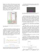
backside, one at bottom of TSV and one at top of wafer frontside. In turn, two main sequences of interference fringes are generated at spectrometer: one is proportional to the wafer total thickness value (TTV) next to via and one is proportional to the remaining Si thickness (RST) below the bottom of via. Typical Fourier Transform (FT) of interferograms used to estimate thicknesses is shown in Figure 1. Depth of TSV was calculated by the difference of two thickness values (TTV and RST). An example of the IR image showing a region of TSVs, and pattern recognition used to align the measurement...
Open the catalog to page 2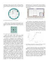
monochrome camera, and color images of detected defects were captured at 10X magnification for review purposes. The location of defective areas for one wafer is shown in Figure 5. interferometry over a 10 µm wide TSV is shown in Figure 7. The measurement was performed by focusing the IR beam down into the Si material, so as to maximize the interference signal intensity. Figure 7: Depth profile over 10 µm wide TSV by IR Interferometry. Fig. 5. Map showing defect locations at frontside of wafer. Off-line review of the inspection results pointed to the presence of scratches, surface particles, and...
Open the catalog to page 3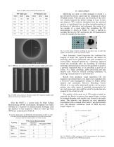
Table I. SEM versus NSX® 320 metrology Since the NSX® is a system ready for High Volume Manufacturing (HVM) environment, throughput was finally estimated as a function of characterization technique used and numbers of sites inspected. Values in wafers per hour (WPH) are summarized in Table II. Table II. throughput by NSX®320: CD performed on 875 via / die over 68 die; Depth profile performed on 6 via/die over 68 die. MACRO INSPECTION PERFORMED ON 100% OF DIES. The analysis of the good set of CD results revealed, as expected, the Bosch via process has opened larger via than the nominal diameter...
Open the catalog to page 4All Onto Innovation Inc. catalogs and technical brochures
 Onto Innovation
19 Pages
 Solid State Technology
6 Pages
 rudolph technologies
1 Page


- Management software solution
- Analysis software solution
- Process software
- Windows software
- Real-time software
- Computer-aided design software
- Design software solution
- Monitoring software solution
- Industrial software
- Inspection system
- Visualization software solution
- Automatic tester
- Automated software
- Industrial tester
- Thickness gauge
- Development software
- Reporting software
- Machine software
- Optimization software
- Automatic inspection system