- Catalogs
- Onto Innovation Inc.
- rudolph technologies
rudolph technologies
1 /1Page

rudolph technologies
1 /1Page
Catalog excerpts
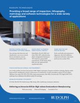
rudolph technologies Providing a broad range of inspection, lithography, metrology and software technologies for a wide variety of applications PROCESS CONTROL AND YIELD MANAGEMENT SOFTWARE (FABWIDE) MACRO DEFECT AUTOMATED INSPECTION (ALL SURFACE) PROBE CARD TEST AND PROCESS ANALYSIS Data mining, fault detection and classification, run-to-run control, factory automation, process modeling; yield analysis, ADC Mask blank, ADi, APi, EBR, Etch clean, OQA, ADC, reduced review; defect management Si interposer, TSV inspection and via depth measurement, 2D/3D bump, eWLB, PMI, post-saw, patterned and unpatterned wafers Probe card build and maintenancealignment, electrical validation, component activation, wire check; probe process analysis-PMI THIN FILM METROLOGY (OPAQUE AND TRANSPARENT) Low-k ILD modulus; Pre/post interconnect CMP; High-k metal gate; Tungsten nucleation and plug; Plating, underbump and RDL metallization; Al and Cu interconnect; Cu seed/barrier; Cu lines; Amorphous carbon; PVD, EP Copper; Diffusion: Gate oxide, NO, ONO, OPO; SiGe; stress measurements; Litho ARCs; Dry/wet etch; CVD; High-k (HfO, ZrO); multi-layer low-k thickness; Thin BEOL metals; CD metrology ADVANCED PACKAGING LITHOGRAPHY FO-WLP, WLCSP, TSV, Solder bump, Pillar bump, RDL, Gold bump, Interposer substrates Delivering an Attractive ROI for High-volume Semiconductor Manufacturing Wafer processing | Advanced Packaging | Assembly & Test
Open the catalog to page 1All Onto Innovation Inc. catalogs and technical brochures
 Onto Innovation
19 Pages
 Solid State Technology
6 Pages
 Use style: paper title
6 Pages


- Analysis software solution
- Process software
- Windows software
- Real-time software
- Computer-aided design software
- Design software solution
- Monitoring software solution
- Industrial software
- Inspection system
- Visualization software solution
- Automatic tester
- Automated software
- Industrial tester
- Thickness gauge
- Development software
- Reporting software
- Machine software
- Optimization software
- Automatic inspection system