- Catalogs
- Onto Innovation Inc.
- Patterning high resolution features through the integration of an advanced lithography system with a novel nozzle-less spray coating technology
Patterning high resolution features through the integration of an advanced lithography system with a novel nozzle-less spray coating technology
1 /7Pages

Patterning high resolution features through the integration of an advanced lithography system with a novel nozzle-less spray coating technology
1 /7Pages
Catalog excerpts
Jack Mach, Corey Shay Applications Engineer Rudolph Technologies Wilmington, MA, USA [email protected] Stuart Erickson President Ultrasonic Systems, Inc. Haverhill, MA, USA [email protected] Gary Smith Regional Manager Sumitomo Chemical Advanced Technologies Phoenix, AZ, USA [email protected] Abstract—As demand for ever more powerful personal handheld devices and advanced computing systems continues to grow, front-end manufacturers have pushed Moore’s Law to the limit and integrated more functionality into their chips while at the same time reducing their physical footprint. Modern chips are now packing more I/O channels into a smaller area than ever before. Being able to interface these devices is becoming more challenging and it is up to the advanced packaging industry to continue to develop technologies and methods to accommodate this requirement, while at the same time, reducing costs and increasing throughput. There are inherent topographical challenges associated with the growth of 2.5D and 3D packaging where chips are placed and interconnected horizontally and vertically. The industry’s drive for cost reduction is building momentum toward large format panels and away from traditional wafers. Larger format panels are exacerbating existing issues, for example, warpage and film stresses. These variables affect the resist coating and exposure steps critical for optimal lithography. Moreover, the current liquid film application methods have encountered obstacles in meeting uniformity requirements for these large panel sizes. Non-uniform film thickness can cause processing variability and poor critical dimension control negatively impacting yield. This paper demonstrates the feasibility of a revolutionary technique in the form of nozzle-less ultrasonic spray technology in conjunction with a next generation advanced packaging lithographic system for the creation of high-density, sub-2.0^m interconnects on a panel format. Performance parameters including resist thickness uniformity, sidewall angle and profile, will be compared and analyzed for this approach and other liquid film application methods. Results from the examination of the efficacy, cost reduction potential of this novel method for high-volume manufacturing will be presented. Keywords-nozzle-less spray; RDL; PLP; WLP; panel; wafer; advanced packaging; stepper; photoresist I. Introduction Demand for more functionality and power in electronic devices continues unabated and will certainly continue into the future. Handheld personal devices, wearables, IoT devices, and even automotive components are all contributing to this momentum. This increased performance demand is accompanied by a seemingly conflicting goal of also reducing the form factor of these modern devices. With front-end-of-line (FEOL) approaching the absolute limits of what can be packed into a chip, it has fallen to the back-end-of-line (BEOL) to shoulder this burden. Advanced packaging is one of the main BEOL suites of technologies where significant gains are still being made. Through the interfacing of chips coming from the FEOL, dedicated packages can be manufactured to meet the performance and dimensional requirements of today’s electronics. Traditionally, advanced packaging has been a predominantly wafer-centric affair, in fan-out wafer level packaging (FOWLP), silicon wafers are diced and reassembled on reconstituted wafers to allow for the redistribution of their I/O channels to other locations and/or chips. In recent years, though, driven in part by the constant need to increase yields and lower cost, panel-level packaging has become an attractive alternative with a growing number of manufacturers investigating and adopting this new medium. This switch has the immediate benefit of mitigating the “square peg, round hole” inefficiency that is inherent in wafer-level packaging. [1] The changeover to panel-level packaging is not without new challenges. Issues that already affect WLP, such as warpage and film stresses become much more pronounced when scaled up to much larger panels. Furthermore, the topographies routinely encountered in modern packages can potentially create film voids when using traditional coating methods. These phenomena create immense difficulty in the crucial lithographic step of coating. Current liquid film application techniques have encountered shortcomings in being able to uniformly coat the larger format panels that are expected in the near future. This non-uniformity directly impacts the exposure step. Any variation in film thickness will result in variable dose, making targeting and maintaining a process window—an especially critical component for lithographic yield—very difficult. Spin coating is a classic film coating method that involves dispensing a puddle on a substrate and then spinning the material to the desired thickness. The resulting film thickness is a function of viscosity of the material, spin speeds used and the duration of the spin. Spin coating is susceptible to particles on the substrate causing “comets”, has trouble conforming to topography and is very wasteful since a large
Open the catalog to page 1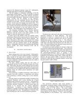
amount of the dispensed material is spun off. Additionally, spinning large panels is physically challenging. Slot die coating is a ubiquitous technology in the flat panel display (FPD) industry. A film of material is extruded from a head, typically the width of the substrate, and drawn across the length of the panel. Thickness is a function of head speed, viscosity and the integrity of the meniscus. Unfortunately, the only similarity between FPD and PLP substrates are the shape. The PLP substrates are much more warped. In some cases, the warpage can exceed 12mm. This presents serious uniformity...
Open the catalog to page 2
pattern distribution comparison between the nozzle-less spray head and a traditional spray head as well as the resultant distribution after a series of overlapping passes. typically experienced in advanced packaging. The stepper lens is achromatized and the installed “filter wheel” provides the user a choice of illumination wavelengths to expose the photoresist layers. Specifically, the user has the ability to image at either “broadband” ghi- (350-450nm), gh- (390 to 450nm) or i-line (365nm) wavelengths. For this study, all exposures were done at i-line. The system utilizes an “on the fly” focus...
Open the catalog to page 3All Onto Innovation Inc. catalogs and technical brochures
 Onto Innovation
19 Pages
 Solid State Technology
6 Pages
 Use style: paper title
6 Pages
 rudolph technologies
1 Page


- Bourn And Koch management software
- Bourn And Koch analysis software
- Bourn And Koch process software
- Bourn And Koch Windows software
- Bourn And Koch real-time software
- Bourn And Koch CAD software
- Bourn And Koch design software
- Bourn And Koch monitoring software
- Bourn And Koch industrial software
- Bourn And Koch inspection system
- Visualization software solution
- Bourn And Koch automated software
- Automatic tester
- Industrial tester
- Bourn And Koch thickness gauge
- Development software
- Bourn And Koch reporting software
- Machine software
- Bourn And Koch optimization software
- Bourn And Koch automatic inspection system