- Catalogs
- Onto Innovation Inc.
- Methodology to Estimate TSV Film Thickness Using a Novel Inline “Adaptive Pattern Registration” Method
Methodology to Estimate TSV Film Thickness Using a Novel Inline “Adaptive Pattern Registration” Method
1 /6Pages

Methodology to Estimate TSV Film Thickness Using a Novel Inline “Adaptive Pattern Registration” Method
1 /6Pages
Catalog excerpts
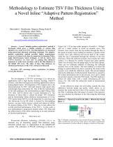
Methodology to Estimate TSV Film Thickness Using a Novel Inline “Adaptive Pattern Registration” Method Shravanthi L Manikonda, Dingyou Zhang, Rudy R. Giridharan, Abner Bello Advanced Module Engineering, GLOBALFOUNDRIES, Malta, USA 12020. [email protected] RUDOLPH Technologies, Budd Lake Township, New Jersey, NJ Figure 1(a). A 0.1ps laser pulse (pump) is focused to ~10x9 m² spot on a wafer surface to create an acoustic wave. The acoustic wave travels from the top surface through the film at the speed of sound. Upon reaching an interface, a portion of the acoustic wave gets reflected and travels back to the surface while the rest is transmitted through the interface to the next film layer. When the reflected acoustic wave reaches the wafer surface, it is detected by another focused laser pulse (probe) which was diverted from the pump pulse by the beam splitter. There are two different methods of detecting the reflected acoustic wave at the surface. The first method is to detect the change in optical reflectivity that is caused by the strain of the acoustic wave called the reflectivity mode. The second method detects the deflection of reflected probe beam that is caused by the surface deformation due to the acoustic wave and is called the position sensitive detection PSD mode. The PSD method is chosen for thick films with a small reflectancee.g.for line arrays. For this work the reflectivity mode of measurement was used. Abstract— A novel “adaptive pattern registration” method is developed which gives a reliable estimate of various film thickness in a wafer level TSV. The film thickness are measured using picosecond ultrasonic metrology technique. The adaptive pattern registration method provides higher measurement accuracy at reduced cycle time in comparison to Scanning WhiteLight Interferometry based technique. It will be shown that TaN/Ta (barrier), Cu Seed and Cu plating film thickness measured at wafer level correlates well to the film thickness at the infield TSV level. The effect of these film thickness on electrical performance of the TSV’s will also be discussed. Keywords—TSV, metrology, pattern registration, Cu plating, trench, film thickness The development of 3D-TSV technology [1] is driven by applications such a high density memory stacking, wide-I/O memory, and other heterogeneous stacking applications such as analog-digital stacks. 3D integration of ICs requires die to die interconnections by TSV with high density, high aspect ratio and through chip connections [2]. One of the key technologies in 3D chip stacking is the electrochemical copper filling of the TSV after TaN/Ta barrier and Cu-seed deposition [3]. The thickness of these films is critical for proper TSV formation and its functionality. Inline thickness measurements of (i) the TSV barrier layer(TaN/Ta) (ii) the deposited Cu seed layer and (iii) bottom-up Cu-via fill which is formed by electroplating process, can give better process control and improved ability for process tuning of the TSV’s. This also in turn affects the overall electrical performance of the TSV’s. In this work, a new methodology is proposed to monitor inline TSV films and the effectiveness of the inline monitoring as an early predictor of electrical performance. II. In the reflectivity mode, the servo-delay controls the time difference between pump and probe, which allows us to measure the round trip travel time of the acoustic wave within the film. Combining this with speed of sound of the material, one can calculate the thickness of the film using the following equation; Thickness = (Speed of sound in the film) x (Round trip transit time) / 2 METHODOLOGY Fig. 1 Schematic representation of picosecond ultrasonic technology. Time delay of probe beam arrival on the wafer surface with respect to pump beam allows measurement of surface reflectivity change as a function of time delay. Picosecond ultrasonic technology (PULSE) [4] is an alternate way of measuring opaque film thickness using ultrashort pulsed laser, as implemented in the MetaPULSE systems. The schematic of PULSE technology is shown in
Open the catalog to page 1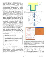
The process flow towards a TSV formation is shown in Fig 2, while Fig 3 shows the TSV formation after the final CMP step. Existing current methodology to measure the TSV thickness of a given wafer is shown in Fig 4 (top). Picosecond ultrasonic technology is used, but the measurement methodology is a blanket type measurements, where equidistant points in a concentric circle pattern are measured, One point is chosen in the innermost ring while 24 points (points 25-49) are chosen in the outermost rings. The number of points and the number of rings can also be varied at any given time and for any...
Open the catalog to page 2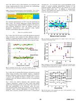
used. The TaN/Ta and Cu film thickness was measured with recipes implementing the above discussed new methodology and the results are as discussed below. deviation (a < 1% is noticed) since a good repeatability of the points is noticed ensuring measurement accuracy of the proposed method. Similar behavior was noticed for Cu seed and Cu plating films also. In addition, to measurement accuracy, this method also reduces cycle time by ~2X as only lower no of points are required. Table 1. Proposed full factorial Design of Experiments(DOE). Three variables - Cu plating thickness, TaN/Ta thickness and...
Open the catalog to page 3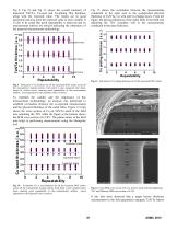
Fig 13 shows the correlation between the measurements conducted in the open area to the as-deposited physical thickness of TaN/Ta, Cu seed and Cu plating layers. From the figure, the physical thickness of the metal films in the field area adjoining the TSV correlates well to the measurements conducted in the open field area. Fig 9, Fig 10 and Fig 11 shows the overall summary of measured TaN/Ta, Cu-seed and Cu-plating film thickness along with the expected value. The results are in good agreement and also meet the expected value of each variable. It is also to be noted that good repeatability...
Open the catalog to page 4All Onto Innovation Inc. catalogs and technical brochures
 Onto Innovation
19 Pages
 Solid State Technology
6 Pages
 Use style: paper title
6 Pages
 rudolph technologies
1 Page


- Management software solution
- Analysis software solution
- Process software
- Windows software
- Real-time software
- Computer-aided design software
- Design software solution
- Monitoring software solution
- Industrial software
- Inspection system
- Visualization software solution
- Automatic tester
- Automated software
- Industrial tester
- Thickness gauge
- Development software
- Reporting software
- Machine software
- Optimization software
- Automatic inspection system