- Catalogs
- Onto Innovation Inc.
- Laser Dark-field Illumination System Modeling for Semiconductor Inspection Applications
Laser Dark-field Illumination System Modeling for Semiconductor Inspection Applications
1 /5Pages

Laser Dark-field Illumination System Modeling for Semiconductor Inspection Applications
1 /5Pages
Catalog excerpts
Laser Dark-field Illumination System Modeling for Semiconductor Inspection Applications Wei Zhou, Darcy Hart and Rajiv Roy - Rudolph Technologies Presented at SPIE Optical System Design Conference, Marseilles, France, September 2011 Dark-field defect inspection is an essential quality control method for the semiconductor fabrication industry, and it is broadly applied for micro particles detection in many fabrication processes, from bare wafer inspection to prior/post litho and etching, to chip dicing and probing, and to final packaging. Diode laser-based DF illumination systems (LDFs) play a critical role in such illumination schemes due to several key factors compared with broadband light sources: compact size and power consumption, low cost relative to high stable output, and most importantly, the unique optical properties that provide additional system flexibility for optimization to the specified applications. A typical LDF illumination system is shown in Fig 1. DF ILLUMINATION APPLICATIONS IN SEMICONDUCTOR DEFECT INSPECTION INDUSTRY AND BEYOND Dark Field illumination by definition inputs light on a 2D target, so the specular reflected output is out of the microscope’s optical collection angle (NA) as shown in Fig 2.1 and 2.2, and a dark image will be formed on the detector plan. Only the edge of a z height variation will scatter the light into more board output angles; partial light will fall into microscope NA and form a signal on the detector plan corresponding to the spatial position on 2D target. Due to the image’s dark background, a strong signal contrast can be achieved by a very small amount of input light. Therefore, DF illumination is a powerful scheme for detecting small variation in height on a 2D surface. This paper reviews the significances of LDF to semiconductor fabrication defect inspection, the fundamental system model is briefly presented, a discussion on the trade-off relationship between the typical system design freedoms and system performance evaluation criteria, followed by the final summary section. Figure 2.1 - Bright-field and dark-field illumination schemes Figure 1 - Typical LDF system Figure 2.2 - Dark-field illumination principle Page 1 of 5 9/11
Open the catalog to page 1
In semiconductor fabrication process, the biggest contributor to yield loss tends to be particles. As the industry embraces more advanced nodes, particle sizes tend to be smaller and more difficult to detect with Bright Field (BF). Other examples of the use of DF in advanced packaging include crater and nodule detection and excessively large bump detection to prevent probe card damage and metal morphology. Even in traditionally easily detectable BF defects caused by residue, due to the properties of newer material DF has been necessary to detect defects such as lifting residue. Specifically,...
Open the catalog to page 2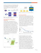
issue when two 3D patterns are small and close enough to be imaged onto the same detector pixel. When the optical path difference is out of phase, the signals will cancel each other and form no signal on detector. Figure 4.2 - Longitudinal and transverse angularity uniformity ANGULAR UNIFORMITY Figure 3 - (top) TEM00 mode laser and projection, (lower) one dimensional flat topped laser projection LDF SYSTEM LEVEL MODELING AND EVALUATION As shown in Fig. 4.1, microscope FOV size is typically much larger than diode laser output spot size, therefore, the laser output beam is typically first focused...
Open the catalog to page 3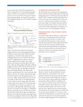
has to be larger than half of FOV longitudinal size which corresponds to 0.5 of normalized propagation distance to FOV size. Less than 0.5 will result laser position to be on top of FOV. The larger the nominal input longitudinal angle, the larger this normalized laser propagation distance has to be ruled by triangular Figure 6 - Longitudinal input angle schematic drawing Figure 8 - System FOV vs input angle and propagation distance Since the intensity distribution along longitudinal direction is always Gaussian distribution, intensity spatial uniformity can be defined as the ratio of minimum...
Open the catalog to page 4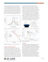
intensity spatial uniformity improves. Therefore, it is a trade-off relationship between photon efficiency and intensity spatial uniformity as shown in Fig 10. In order to achieve 80% intensity spatial uniformity, the input angle cannot be larger than 4 degrees input angle, unless to defocus spot size to extremely large, which in turn will push laser much further away from FOV and result in much smaller photon efficiency. away from microscope FOV quickly, therefore photon efficiency drops accordingly, so does photon efficiency. Lager on-wafer laser spot size can help with this issue. This simulation...
Open the catalog to page 5All Onto Innovation Inc. catalogs and technical brochures
 Onto Innovation
19 Pages
 Solid State Technology
6 Pages
 Use style: paper title
6 Pages
 rudolph technologies
1 Page


- Bourn And Koch management software
- Bourn And Koch analysis software
- Bourn And Koch process software
- Bourn And Koch Windows software
- Bourn And Koch real-time software
- Bourn And Koch CAD software
- Bourn And Koch design software
- Bourn And Koch monitoring software
- Bourn And Koch industrial software
- Bourn And Koch inspection system
- Visualization software solution
- Bourn And Koch automated software
- Automatic tester
- Industrial tester
- Bourn And Koch thickness gauge
- Development software
- Bourn And Koch reporting software
- Machine software
- Bourn And Koch optimization software
- Bourn And Koch automatic inspection system