- Catalogs
- Onto Innovation Inc.
- Improving the Accuracy of Bump Height and Coplanarity Measurement
Improving the Accuracy of Bump Height and Coplanarity Measurement
1 /4Pages

Improving the Accuracy of Bump Height and Coplanarity Measurement
1 /4Pages
Catalog excerpts

SEMICONDUCTORS PACKAGING • MEMS • LEDS • DISPLAYS DECEMBER 2016 SEMICONDUCTORS PACKAGING • MEMS • LEDS • DISPLAYS DECEMBER 2016 Insights for El ^ MRAM Takes State NOLOGY ctronics Manufacturing www.solid-state.co MEDIA
Open the catalog to page 1
Improving the accuracy of bump height and coplanarity measurement SCOTT BALAK , Rudolph Technologies, Inc., Bloomington, MN A new approach to bump height measurements uses an interferometric technique to accurately measure bump height and PL thickness older bumps are used to connect die to various package components in advanced packaging processes. Bump height and coplanarity are critical to ensuring reliable connections. A bump that is not high enough will not connect, while one that is too tall may prevent connection by neighboring bumps or even damage an electrical tester’s probing card. Measuring...
Open the catalog to page 2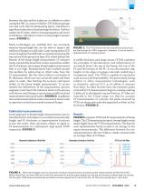
between the chip and the substrate. In addition to eliminating the IMC as a source of failure, UFI reduces package cost and cycle time by eliminating layers, and allows a significant reduction in final package thickness. Unfortunately, the PL layer, which is semitransparent and varies in thickness, introduces errors in bump height measurements (FIGURE 1). Many technologies are available that can accurately measure bump height but are too slow to inspect the millions of bumps on a full wafer. Laser triangulation (LT) is fast enough but has difficulty accurately measuring the top surface of the...
Open the catalog to page 3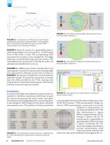
FIGURE 7. Corrected LT bump height measurements from a full wafer 100% inspection. FIGURE 5. A comparison of VTSS and LT bump height measurements shows a consistent offset. In this example the LT measurement exceeds the more accurate VTSS measurement by an average of 2.123μm. FIGURE 6 shows the results of a repeatability study in which bump heights were measured for ~12,000 bumps from 13 dies across a wafer. The accompanying wafer map shows the locations of the sampled die. 3D height inspection was performed using 5µm spot sensors. The repeatability test was dynamic, meaning the wafer was unloaded...
Open the catalog to page 4All Onto Innovation Inc. catalogs and technical brochures
 Onto Innovation
19 Pages
 Solid State Technology
6 Pages
 Use style: paper title
6 Pages
 rudolph technologies
1 Page


- Management software solution
- Analysis software solution
- Process software
- Windows software
- Real-time software
- Computer-aided design software
- Design software solution
- Monitoring software solution
- Industrial software
- Inspection system
- Visualization software solution
- Automatic tester
- Automated software
- Industrial tester
- Thickness gauge
- Development software
- Reporting software
- Machine software
- Optimization software
- Automatic inspection system