- Catalogs
- Onto Innovation Inc.
- The Impact of Backside Particle Contamination
The Impact of Backside Particle Contamination
1 /1Page

The Impact of Backside Particle Contamination
1 /1Page
Catalog excerpts
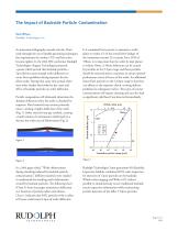
The Impact of Backside Particle Contamination Matt Wilson Rudolph Technologies, Inc. As immersion lithography extends into the 32nm node through the use of double patterning techniques, the requirements for overlay, CDU and focus also become tighter. In the 2006 SPIE conference Rudolph Technologies (August Technology) presented a poster which proved that backside particles < 5μm did not cause enough wafer deflection to create focus problems during exposure for the 65nm node. During that same time period, there were other studies that looked at the cause and effect of backside particles on wafer deflection. Particle composition will ultimately determine the absolute deflection when the wafer is chucked for exposure. Hard material may remain primarily intact, creating a higher deflection of the wafer (Fig. 1). Softer material may get crushed, creating a small volume of contaminant which leads to a shorter, but wider area of deformation (Fig. 2). It is considered best practice to maintain a wafer plane to within 1/3 of the overall DOF budget of the immersion scanner. If a scanner has a DOF of 150nm, it is important that the wafer be kept planar to within 50nm. A 50nm deflection can be caused by particles in the 3-5μm range and those particles should be removed prior to exposure to ensure optimal performance across all areas of the wafer. An additional threat from particles in the 3-10μm range is that they can adhere to the exposure chuck, creating defocus problems for subsequent wafers. This type of scanner contamination will require cleaning and can also lead to significant yield loss if not detected immediately. In a 2006 paper titled, “Wafer deformations during chucking induced by backside particle contamination”, different materials were studied to understand the resulting wafer deformation created by backside particles. The following chart (Chart 1) from that paper summarizes deflection as a function of particle radius and volume. Chart 1 indicates that SiO2 particles with a radius of 10 μm could create 0.1μm of wafer deflection. Rudolph Technologies’ latest generation B30 Backside Inspection Module combines BF/DF color inspection for detection of >3μm particles on the backside. Whole wafer imaging and Wafer ADC make it possible to simultaneously secure traditional backside macro inspection information while maintaining particle detection of the killer 5-10μm particles.
Open the catalog to page 1All Onto Innovation Inc. catalogs and technical brochures
 Onto Innovation
19 Pages
 Solid State Technology
6 Pages
 Use style: paper title
6 Pages
 rudolph technologies
1 Page


- Bourn And Koch management software
- Bourn And Koch analysis software
- Bourn And Koch process software
- Bourn And Koch Windows software
- Bourn And Koch real-time software
- Bourn And Koch CAD software
- Bourn And Koch design software
- Bourn And Koch monitoring software
- Bourn And Koch industrial software
- Bourn And Koch inspection system
- Visualization software solution
- Bourn And Koch automated software
- Automatic tester
- Industrial tester
- Bourn And Koch thickness gauge
- Development software
- Bourn And Koch reporting software
- Machine software
- Bourn And Koch optimization software
- Bourn And Koch automatic inspection system