- Catalogs
- Onto Innovation Inc.
- All-surface Inspection for 3D-interconnects and TSV Manufacturing
All-surface Inspection for 3D-interconnects and TSV Manufacturing
1 /5Pages

All-surface Inspection for 3D-interconnects and TSV Manufacturing
1 /5Pages
Catalog excerpts
APPLICATION NOTE All-surface Inspection for 3D-interconnects and TSV Manufacturing Rolf Shervey (presented at iwlpc 2009) ABSTRACT The need to inspect the topside, edge/bevel and backside of wafers at various stages of the semiconductor manufacturing process has been driven by device manufacturers continuing the push to 100% wafer-surface utilization for active die. As a result, the wafer-edge exclusion is becoming a thing of the past. With requirements for improving yield, thereby reducing costs, coming to the forefront, processing challenges are simultaneously increasing. The effect of adding knowledge about topside, bevel and backside-specific process phenomenon can be utilized not only in killer defect detection, but also in process improvement that ultimately drives yield improvement. Once-new processes such as immersion lithography and deposition of high-k dielectric films have driven the development of wafer edge inspection technologies. As these processes become mainstream to semiconductor manufacturing, the next big drivers for continuous improvement inspection and metrology equipment (and the application of that equipment) will include the 3D-interconnects (3DIC) initiatives. Interconnects are one of the industry’s most difficult challenges: they involve depositing metal into deep and narrow microscopic holes etched into a chip. 3DIC has specific needs for yield-enhancing information and analysis which can be addressed by the next generation of all-surface inspection equipment. Wafer-Level and Chip-Scale Packaging brought the concept of re-introducing a “back-end wafer” back into the front-end process for RDL deposition and subsequent steps, and this is being seen again in the 3DIC/TSV development path. There is much key learning in inspection and metrology that can be applied to these parallels, which if shared and applied correctly will result in a shorter learning curve as 3DIC/TSV processes become standardized. 3D interconnects are important because of the push towards faster, more functional devices that are simultaneously smaller, and more power efficient. Connecting chips with discrete functions in a highly parallel way, and using the same PCB real-estate is the end goal. For example, by integrating memory above a processor die with a 1,000 “pins” (or TSVs) parallel connection can reduce power consumption in the interconnect to less than 1/10th that of a conventional interconnect.1 TSVs may be the vehicle the industry uses to extend Moore’s law by allowing us to sidestep the issue of shrinking the transistor pitch altogether. TSVs promise the best advantages of System-on-Chip (SoC) and System-in-Package (SiP) together while achieving the optimum balance of functionality, low cost, and the shortest time to market among all serious alternatives. Through-Silicon Vias (TSVs) will be the 3D interconnects’ method of choice for future generations of devices because of the many advantages offered, chief among them being the higher densities of Figure 1 - TSV cross-section (SEM interconnects possible. This image) results in faster devices with lower power consumption. There is also the ability to manufacture the interconnects in-situ or along with die level packaging processes, instead of requiring separate device-level integration at wire bonding. This paper discusses the applications for inspecting all surfaces of semiconductor wafers during various steps in the 3D interconnects and TSV manufacturing cycle. Inspections were performed on a Rudolph Technologies AXi™-935 E30/B30 Advanced Macro-Defect Inspection system at SEMATECH’s
Open the catalog to page 1
wafer-to-wafer (WtW) 3D interconnect line at the College of Nanoscale Science and Engineering (CNSE), University at Albany, State University of New York (SUNY). Examples of inspections taking place on the front, edge/bevel and backside of the wafer will be shown and the potential yield saving impacts discussed. what is “bad” and “good” based on a number of flexible variables that can be controlled by the equipment engineer. For instance, certain contrast levels or feature shapes. By allowing flexible and subjective variables to be defined which adjust the inspection results, automated inspection...
Open the catalog to page 2
Bevel inspection is equally important to 3D interconnects manufacturing. HANDLING OF BONDED WAFERS Because the wafers are bonded during the 3D process, it is important that the equipment (including the robotic wafer handler) is able to handle a ~1550 micron thick wafer pair, equivalent to two standard SEMI M1 300 mm diameter wafers at 775± 25 micron total thickness each.2 Because this is not yet common throughout the industry, we found that there were several challenges to be addressed specific to handling bonded wafers. Adjustments to the cassette mapping were necessary so that the robot would...
Open the catalog to page 3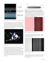
Figure 8 - Diagram of edge-trimmed, thinned wafer on carrier wafer. Edge-Top Inspection of Wafer After Trimming Process As the wafer edge becomes very thin - like a knife edge during grinding, it has a chance of breaking. To avoid this, the top wafer can be trimmed prior to the thinning step (figure 8). The edge trimming process can be monitored for process problems such as cracking or chipping. Figure 6 - Edge-normal image of bonded wafer pairs showing defect in bond area In the bonding process there is a chance for foreign material (FM) to be introduced into the bond area, or between the wafers....
Open the catalog to page 4
Backside Inspection of Wafers in Bond Processes The most often neglected area on a wafer is the backside. In typical wafer processing, the backside of a wafer has This paper demonstrated the value of performing inline automated inspections during 3D interconnects manufacturing by showing that key defects of interest are captured after various processing steps. The bonding of wafers, and the unique challenges that accompany it, are unique to 3D interconnects and demand new equipment and new methods to address the emerging inspection and metrology requirements. The fact that these wafers must be...
Open the catalog to page 5All Onto Innovation Inc. catalogs and technical brochures
 Onto Innovation
19 Pages
 Solid State Technology
6 Pages
 Use style: paper title
6 Pages
 rudolph technologies
1 Page


- Management software solution
- Analysis software solution
- Process software
- Windows software
- Real-time software
- Computer-aided design software
- Design software solution
- Monitoring software solution
- Industrial software
- Visualization software solution
- Automatic tester
- Automated software
- Industrial tester
- Thickness gauge
- Development software
- Reporting software
- Machine software
- Optimization software
- Automatic inspection system