- Catalogs
- Onto Innovation Inc.
- Advanced Packaging Lithography and Inspection Solutions for Next Generation FOWLP-FOPLP Processing
Advanced Packaging Lithography and Inspection Solutions for Next Generation FOWLP-FOPLP Processing
1 /6Pages

Advanced Packaging Lithography and Inspection Solutions for Next Generation FOWLP-FOPLP Processing
1 /6Pages
Catalog excerpts

Advanced Packaging Lithography and Inspection Solutions for Next Generation FOWLP-FOPLP Processing Keith Best, Gurvinder Singh, and Roger McCleary Rudolph Technologies, Inc. 16 Jonspin Rd. Wilmington, MA 01887, U.S.A. Ph: 978-253-6200; Fax: 978-658-6349 Email: [email protected] Abstract For more than 50 years the semiconductor industry has pursued Moore’s law, continuously improving device performance, reducing cost, and scaling transistor geometries down to where advanced CMOS has reached beyond the 10nm technology node. The commensurate increase in I/O count has created many challenges for device packaging which hitherto was considered low cost with simple solutions. It was once thought that old backend foundry lithography steppers could be used to address the new packaging requirements; which was true whilst the substrates remained in the traditional 300mm Silicon format. The recent unprecedented rapid growth in Fan-out Wafer Level Packaging (FOWLP) applications has introduced a more complicated landscape of process challenges, with no restriction on substrate format, where cost is the main driver and high yields are mandatory. This paper discusses the lithography process challenges that have ensued from disruptive FOWLP, and more recently the paradigm shift to Fan-out Panel Level Packaging (FOPLP). The work reports on lithography solutions for CD control over topography and high aspect ratio imaging of 2µm line/space RDL. In addition, the introduction of new inspection capabilities for defects and metrology is reported for both wafers and panels. The increase in lithography productivity and cost reduction provided by FOPLP is also discussed with production examples. Key words Fluorescence, FOWLP, Inspection, Panel, Stepper, Thick Resist presents a number of manufacturing and process control challenges. These includes chip placement on the carrier, molding, via reveal, Re-distribution layer (RDL) fabrication and final ball placement. OSATs are also continuously pushing for smaller line space pitch RDL on these fan-out packages. This drives the need for high resolution lithography and inspection systems that are capable of handling, patterning and inspecting large panels. In addition, BEOL processing induces stress to the substrates which results in significant warpage on both wafers and the panels, this presents additional challenges to not only handling but also detection of sub-micron defects. I. Introduction With the ever increasing pressure to reduce costs and improve productivity, Out-Sourced Assembly and Test (OSAT) companies continuously make changes to their processing methods and substrate formats. In particular, moving from Silicon to reconstituted Epoxy Mold Compound (EMC) wafers has enabled the OSATs to become independent of substrate size & shape. Moreover, this freedom has enabled the use of large area panels which leverage economy of scale to further reduce costs, Fig. 1. shows the significant increase in die as a function of substrate size. Larger panel based substrates in back-end packaging processes promise significant reductions in cost per package. A 30-40% cost reduction of the panel can be achieved relative to round 300mm wafer fan-out. In addition to the economic benefit, panel fan-out packaging enables the industry to move to larger fan-out packages with multiple chip integration. However, panel scale fan-out processing
Open the catalog to page 1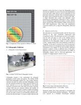
maintain overlay from layer to layer the lithography system also has the capability to correct for scale and magnification across the larger image field as well as compensate for die placement inaccuracy realized with reconstituted panels by the gantry used to populate the panel or curing of the EMC. A single telecentric lens system with adjustable reticle positioning for magnification, trapezoid in x and y, rotation, and xy translation is appropriate to achieve overlay with the larger exposure field. This capability enables corrections for intra field magnification, scale, theta and compliments...
Open the catalog to page 2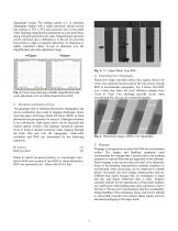
lithography system. The JetStep system is a 2x reduction lithography stepper with a single telecentric optical system that exposes a 59.4 x 59.4 mm exposure area on the panel while enabling magnification adjustment on a per panel basis along with grid corrections for scale. Magnification and scale can be corrected, up to ±400 ppm or 11.88 µm of correction from center to edge of exposure field (Fig. 4). Distortion is tightly controlled within <0.1µm of distortion over the magnification and scale adjustment range. Fig. 5. 5:1 Aspect Ratio, 2µm RDL D. Patterning Over Topography Panels have larger...
Open the catalog to page 3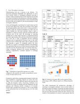
F. Panel Throughput Advantage Manufacturing costs are a concern in any industry. For advanced packaging lithography the opportunity to move from circular wafers to rectangular substrates provides a means to reduce manufacturing costs by utilizing tool sets that have been developed for the production of flat panel displays, printed circuit boards and solar panels. All use manufacturing processes that can be applied to advanced packaging on large rectangular substrates. Front-end lithography is performed on round wafers and die are lost at the edge of the wafer due to portions of the square die...
Open the catalog to page 4
number of die populated on a wafer, resulting in a >89% productivity advantage when exposing on panels instead of wafers. G. Inspection Solutions To inspect warped wafer or panels for defects, Rudolph Technologies has developed Firefly™ Inspection system with ClearFind™ technology. ClearFind™ technology incorporates a dual focus system - a coarse z focus system that allows the optics to stay in the optimum focus range while a fine focus system which continuously measures the local topography as it scans the panel and adjusts focus automatically. This unique patented methodology allows the user...
Open the catalog to page 5
R. Dudley, D. Marx, R. Roy, D. Grant, M. Wilson, and S. Balak, “Inspection and metrology solutions from TSV through reveal for high volume manufacturing”, Rudolph Technologies IMAPS 47th International Symposium on Microelectronics, October 2013. R. Roy, “Front-end-ization of the back-end”, Rudolph Technologies IMAPS 47th International Symposium on Microelectronics, October 2013 N. Devanciard [CEI-Leti] and Dario Alliata [Rudolph Technologies, Inc.], “Combining defect detection/metrology to accelerate microbump/pillar fabrication, (Periodical style-submitted for publication),” Chip Scale Review,...
Open the catalog to page 6All Onto Innovation Inc. catalogs and technical brochures
 Onto Innovation
19 Pages
 Solid State Technology
6 Pages
 Use style: paper title
6 Pages
 rudolph technologies
1 Page


- Management software solution
- Analysis software solution
- Process software
- Windows software
- Real-time software
- Computer-aided design software
- Design software solution
- Monitoring software solution
- Industrial software
- Visualization software solution
- Automatic tester
- Automated software
- Industrial tester
- Thickness gauge
- Development software
- Reporting software
- Machine software
- Optimization software
- Automatic inspection system