- Catalogs
- Onto Innovation Inc.
- Acoustic Metrology for Fine Pitch Microbumps in 3DIC
Acoustic Metrology for Fine Pitch Microbumps in 3DIC
1 /5Pages

Acoustic Metrology for Fine Pitch Microbumps in 3DIC
1 /5Pages
Catalog excerpts
M. Mehendale, J. Chen, J. Dai, R. Mair, M Kotelyanskii, P. Mukundhan Rudolph Technologies Budd Lake, NJ, USA Manjusha. mehendale@rudolphtech. com Abstract - The continuing shift to 3D integration requires formation of electrical interconnects between multiple vertically stacked Si devices to enable high speed, high bandwidth connections. Microbumps and through silicon vias (TSV) enable the high-density interconnects for die-to-die and die-to-wafer stacking for different applications. In this paper, we present acoustic metrology techniques for the measurement of multi-layer microbumps. One of the techniques, PULSE™ technology, is a very well-established mature solution for metal film thickness measurements. Repeatability and accuracy of the measurements more than adequately meets the process requirements. We also present a second nondestructive acoustic metrology for measuring taller copper pillars (> 30pm). Keywords: microbump, acoustic metrology, picosecond ultrasonics, advanced packaging I. Introduction With the approaching limitation of Moore’s law scaling, the semiconductor industry has turned to advanced packaging technologies to meet high-performance computing needs. 3D integration and formation of electrical interconnects between multiple vertically stacked Si devices have enabled high speed, high bandwidth connections. Microbumps and through silicon vias (TSV) are the key architectural elements for die-to-die and die-to-wafer stacking as they improve performance of the complete system. Typical solder height is 15-30pm in Cu pillars and it is expected to scale down to less than 10 pm in 20 pm pitch interconnections. Solder based, fine pitch, microbump connections are preferred mainly due to lower bonding temperature compared with Cu-to-Cu thermo-compression bonding. However, with reducing bump dimensions, several critical reliability issues arise such as the small solder volume transformation and conversion to complete intermetallic compound (IMC), during thermocompression bonding. Studies have also shown that for a 20pm microbump the current density can reach values that are significantly higher than the threshold value of Sn electromigration (EM) and the failure mechanism in microbumps are different from traditional flip chip bump. Two main EM failure mechanisms are reported: void propagation along the IMC/solder interface and the dissolution of under-bump-metallization (UBM) [1-4]. T. W. Murray Department of Mechanical Engineering University of Colorado 427 UCB, Engineering Center Boulder, CO, USA From a bump processing standpoint, it is common to plate multi-metal films on the same equipment to minimize oxidation between metal depositions as well as to increase production flexibility and minimize risks due to equipment downtimes. Thickness information on microbumps (<30pm) are currently obtained from either step height measurements, X-ray techniques or cross-section microscopy. While these tools provide information in the form of indirect thickness, or Ag concentration in solder, they cannot be adopted for inline monitoring in a high-volume manufacturing environment. The scaling microbumps also require a technology with a small measurement spot size to be able to position and measure on individual microbumps. Small spot (~10pm) picosecond ultrasonics (PULSE™) is well established in wafer fabs for metal film thickness measurement. The capability of the technique to measure UBM and redistribution layers (RDL) has been previously reported [6]. In this paper, we review microbump characterization using this technique. Additionally, we also used a second independent acoustic metrology tool to validate the results in this thickness regime and as an extension of capability of the technique for taller pillars. II. Methodology Picosecond ultrasonic metrology is a pump-probe technique. We have previously [6] discussed at length the underlying principle and measurement setup of the standard configuration. Interested readers are referred to those publications. In the standard configuration, the pump beam is modulated at 5.5MHz, probe beam is unmodulated and the signal is demodulated at the same frequency as the pump beam modulation frequency. The rough surface of the films scatter the measurement beams excessively, thus increasing the noise and reducing the overall signal to noise ratio (SNR). To overcome some of the challenges of the rough surface in the standard configuration, site averaging is performed by adding additional measurement sites (mini maps) to average the local surface roughness with impact to throughput. In this study, we used a dual modulation setup (Fig 1). The pump beam was modulated at 5MHz, the probe beam was modulated at 0.5MHz and the signal demodulated at 5.5MHz. Any scattering from both pump and probe beams was filtered out. The technique is currently capable of measuring films from 40A to 30pm, depending on materials. This method is well suited for measuring the microbumps,
Open the catalog to page 1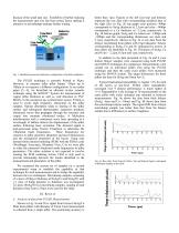
because of the small spot size. Feasibility of further reducing the measurement spot size has been tested, hence making it attractive as microbumps undergo further scaling. Fig. 1. Modified picosecond ultrasonic configuration with dual modulation. The PULSE technique is currently limited to 30µm. However, to measure taller pillar bumps >30µm up to 100µm or so requires a different configuration. In an earlier paper [5, 6], we described an alternate in-line acoustic technique using the SONUS™ System for measurement of copper pillar thickness as well as void detection in TSV. Briefly, in the second...
Open the catalog to page 2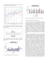
Fig. 2b. Thermal background-subtracted data from the bi-layer films. Modeled fit (black) to measured data (green) shown. Fig. 4b. Load/unload repeatability of tri-layer measured simultaneously. B. Analysis of data from the SONUS System Fig. 3a. Raw data from tri-layer bump stack. The different traces represent multiple sites across the wafer. Variations in echo positions correspond to cross wafer variation. Fig. 3b. Thermal background subtracted data with echo positions from the tri-layer identified. The three arrows correspond to SnAg/Ni/Cu, respectively. Fig. 4a. Load/unload repeatability of...
Open the catalog to page 3All Onto Innovation Inc. catalogs and technical brochures
 Onto Innovation
19 Pages
 Solid State Technology
6 Pages
 Use style: paper title
6 Pages
 rudolph technologies
1 Page


- Bourn And Koch management software
- Bourn And Koch analysis software
- Bourn And Koch process software
- Bourn And Koch Windows software
- Bourn And Koch real-time software
- Bourn And Koch CAD software
- Bourn And Koch design software
- Bourn And Koch monitoring software
- Bourn And Koch industrial software
- Bourn And Koch inspection system
- Visualization software solution
- Bourn And Koch automated software
- Automatic tester
- Industrial tester
- Bourn And Koch thickness gauge
- Development software
- Bourn And Koch reporting software
- Machine software
- Bourn And Koch optimization software
- Bourn And Koch automatic inspection system