FT8010 Reset Timer with Configurable Delay
FT8010 Reset Timer with Configurable Delay
- Configurable delay times of 7.5 or 11.25 seconds.
- Primary and secondary input reset pins.
- Push-pull and open-drain output pins.
- Operates from 2.0V to 5.0V.
Catalog excerpts

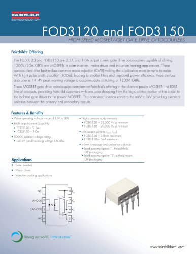
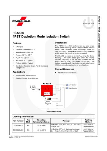
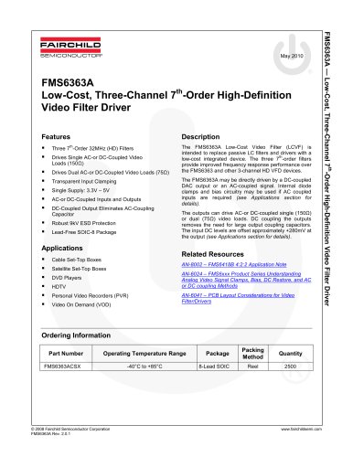
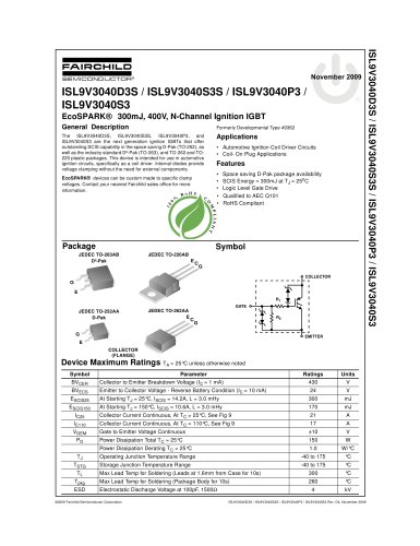
December 2010 © 2009 Fairchild Semiconductor Corporation www.fairchildsemi.com FT8010 • Rev. 1.0.3 FT8010 — Reset Timer with Configurable Delay Time FT8010 Reset Timer with Configurable Delay Time Features .. Long Delay Configurable to 7.5 or 11.25 Seconds .. Primary and Secondary Input Reset Pins .. Push-Pull and Open-Drain Output Pins .. 2.0V to 5.0V Operation .. Packaged in 10-Lead UMLP (1.4mm x 1.8mm) and 8-Lead MLP (2.0mm x 2.0mm) Packages Description The FT8010 is a timer for resetting a mobile device where long reset times are needed. The long time delay helps avoid unintended resets caused by accidental key presses. Two delays can be selected by hard-wiring the DSR pin: 7.5 ±20% seconds or 11.25 ±20% seconds. The FT8010 has two identical inputs for single or dual switch resetting capability. The device has two outputs: a push-pull output with 0.5mA drive and an open-drain output with 0.5mA pull-down drive. FT8010 draws minimal ICC current when inactive and functions over a wide 2.0V to 5.0V power supply range. Ordering Information Part Number Operating Temperature Range Package Packing Method FT8010UMX -40°C to +85°C 10-Lead Ultrathin MLP, 1.4 x 1.8 x 0.55mm Package, 0.40mm Pitch 5000 Units Tape and Reel FT8010MPX -40°C to +85°C 8-Lead, MLP 2.0 x 2.0 x 0.8mm Package, 0.5mm Pitch 3000 Units Tape and Reel
Open the catalog to page 1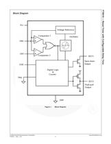
© 2009 Fairchild Semiconductor Corporation www.fairchildsemi.com FT8010 • Rev. 1.0.3 2 FT8010 — Reset Timer with Configurable Delay Time Block Diagram Figure 1. Block Diagram
Open the catalog to page 2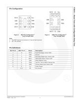
© 2009 Fairchild Semiconductor Corporation www.fairchildsemi.com FT8010 • Rev. 1.0.3 3 FT8010 — Reset Timer with Configurable Delay Time Pin Configuration Figure 2. MLP Pin Configuration(1) (Top Through View) Figure 3. UMLP Pin Configuration(2) (Top Through View) Note: 1. The DAP may be a no connect or it may be tied to ground. 2. NC = No connect Pin Definitions MLP Pin # UMLP Pin # Name Description 1 10 RST2 Push-Pull Output, Active HIGH 2 1 GND Ground 3 2 /SR1 Secondary Reset Input, Active LOW 4 3 /RST1 Open-Drain Output, Active LOW 5 5 DSR Delay Selection Input 6 6 TRIG Test Pin, Tied to GND...
Open the catalog to page 3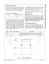
© 2009 Fairchild Semiconductor Corporation www.fairchildsemi.com FT8010 • Rev. 1.0.3 4 FT8010 — Reset Timer with Configurable Delay Time Functional Description The FT8010 reset timer uses an internal oscillator and a two-stage, 21-bit counter to determine when the output pins switch. Time N is set by the hard-wired logic level of the DSR pin. N is either 7.5 ±20% seconds for DSR=LOW or 11.25 ±20% seconds for DSR=HIGH. Table 1. FT8010 Truth Table DSR Reset Timer ( +-20% ) 0 7.5s 1 11.25s The two input pins, /SR0 and /SR1, drive voltage comparators that compare the voltage on the input with the...
Open the catalog to page 4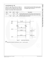
© 2009 Fairchild Semiconductor Corporation www.fairchildsemi.com FT8010 • Rev. 1.0.3 5 FT8010 — Reset Timer with Configurable Delay Time Long Duration (tW > N) In this case, inputs /SR0 and /SR1 are LOW for a duration, tW, which is longer than time N. When an input goes LOW, the internal timer starts counting. After time N, the outputs switch and the timer stops counting. The input goes HIGH sometime after N seconds. When the input goes HIGH, the timer resets and the outputs switch back to their original state after a propagation delay (see Figure 5). /SR0 /SR1 /RST1 RST2 Description L The timer...
Open the catalog to page 5
© 2009 Fairchild Semiconductor Corporation www.fairchildsemi.com FT8010 • Rev. 1.0.3 6 FT8010 — Reset Timer with Configurable Delay Time Absolute Maximum Ratings Stresses exceeding the absolute maximum ratings may damage the device. The device may not function or be operable above the recommended operating conditions and stressing the parts to these levels is not recommended. In addition, extended exposure to stresses above the recommended operating conditions may affect device reliability. The absolute maximum ratings are stress ratings only. Symbol Parameter Conditions Min. Max. Unit VCC Supply...
Open the catalog to page 6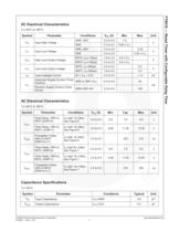
© 2009 Fairchild Semiconductor Corporation www.fairchildsemi.com FT8010 • Rev. 1.0.3 7 FT8010 — Reset Timer with Configurable Delay Time DC Electrical Characteristics TA=-40°C to +85°C. Symbol Parameter Conditions VCC (V) Min. Max. Unit VIH Input High Voltage /SR0, /SR1 2.0 to 5.0 1.2 V DSR 2.0 to 5.0 0.65 x VCC VIL Input Low Voltage /SR0, /SR1 2.0 to 5.0 0.32 V DSR 2.0 to 5.0 0.25 x VCC VOH High Level Output Voltage RST2, IOH=-100ìA 1.8 to 3.0 0.8 x VCC V RST2, IOH=-500ìA 3.0 to 5.0 0.8 x VCC VOL Low Level Output Voltage RST2, IOL=500ìA 2.0 to 5.0 0.3 V /RST1, IOL=500ìA 1.8 to 5.0 0.3 IIN Input...
Open the catalog to page 7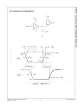
© 2009 Fairchild Semiconductor Corporation www.fairchildsemi.com FT8010 • Rev. 1.0.3 8 FT8010 — Reset Timer with Configurable Delay Time AC Test Circuit and Waveforms Figure 6. /RST1 Output
Open the catalog to page 8
© 2009 Fairchild Semiconductor Corporation www.fairchildsemi.com FT8010 • Rev. 1.0.3 9 FT8010 — Reset Timer with Configurable Delay Time AC Test Circuit and Waveforms (Continued) Figure 7. RST2 Output
Open the catalog to page 9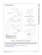
© 2009 Fairchild Semiconductor Corporation www.fairchildsemi.com FT8010 • Rev. 1.0.3 10 FT8010 — Reset Timer with Configurable Delay Time Physical Dimensions Figure 8. 10-Lead Ultrathin MLP, 1.4 x 1.8 x 0.55mm Package Package drawings are provided as a service to customers considering Fairchild components. Drawings may change in any manner without notice. Please note the revision and/or date on the drawing and contact a Fairchild Semiconductor representative to verify or obtain the most recent revision. Package specifications do not expand the terms of Fairchild’s worldwide terms and conditions,...
Open the catalog to page 10
© 2009 Fairchild Semiconductor Corporation www.fairchildsemi.com FT8010 • Rev. 1.0.3 11 FT8010 — Reset Timer with Configurable Delay Time Physical Dimensions (Continued) Figure 9. 8-Lead, Molded Leadless Package (MLP), 2.0 x 2.0 x 0.8mm Package drawings are provided as a service to customers considering Fairchild components. Drawings may change in any manner without notice. Please note the revision and/or date on the drawing and contact a Fairchild Semiconductor representative to verify or obtain the most recent revision. Package specifications do not expand the terms of Fairchild’s worldwide...
Open the catalog to page 11All Onsemi catalogs and technical brochures
 FOD8383 2.5 A Output Current
18 Pages
 Logic SELECTION GUIDE
12 Pages
 Automotive Solutions Guide
8 Pages
 Motor Drive Solution Guide
20 Pages
 Mobile Solutions Guide
40 Pages
 AUTOMOTIVE SOLUTIONS
16 Pages
 Power Solutions Guide
60 Pages
 STANDARD PRODUCTS GUIDE
72 Pages


Archived catalogs
 Mobile overview
4 Pages
 Analog switch & interface
12 Pages
 TinyLogic® Product Overview
4 Pages
 3:1 Analog Switch Products
2 Pages
 USB Multimedia Switches
2 Pages
 Optocoupler Solutions
24 Pages
 LED LIGHTING SOLUTIONS
16 Pages
 Motor DRIVE solutions
32 Pages
 DIGITAL DISPLAY SOLUTIONS
36 Pages
 RENEWABLE ENERGY SOLUTIONS
32 Pages
 FGPF4536 360V, PDP IGBT
8 Pages
 FSAR001B AC-DC Linear Regulator
12 Pages
 Fairchild - Power solutions
52 Pages


- Position transducer
- Wireless module
- Potentiometer
- Onsemi transistor
- Industrial position sensor
- Onsemi switching transistor
- Angular position sensor
- Motor driver
- Onsemi bipolar transistor
- Digital position sensor
- DC motor motor driver
- Mechanical position sensor
- DRAM memory module
- Control potentiometer
- Signal preamplifier
- CMOS image sensor
- Applications preamplifier
- IGBT transistor
- Onsemi audio transistor
- Inductive position sensor