


FSHDMI08 Wide-Bandwidth Differential Signaling HDMI Switch
FSHDMI08 Wide-Bandwidth Differential Signaling HDMI Switch
The FSHDMI08 is a low-voltage, wide-bandwidth HDMI switch with DDC and CEC multiplexer designed by Fairchild Semiconductor. It supports data rates up to 1.65Gbps per channel, suitable for UXGA resolution, and is used in applications like LCD TVs, DVD players, set-top boxes, and notebooks with multiple digital video interfaces.
Features
- Non-adjacent channel crosstalk of -25db at 1.65Gbps
- Low signal loss with -1.5dBg attenuation at 1.65Gbps
- Fast turn-on/off time (<6ns)
- 8kV ESD protection
- Low skew: Intra-pair <90ps, Inter-pair <150ps
- Low power consumption: 1µA maximum
Applications
- XGA and 720p DVI and HDMI video source selection
Specifications
- Supply Voltage: TMDS Channels -0.5 to 4.6V, DDC 5V -0.5 to 6.0V
- Operating Temperature: -40 to +85°C
- Maximum Junction Temperature: +150°C
- Storage Temperature Range: -65 to +150°C
Electrical Characteristics
- Clamp Diode Voltage: -1.2V
- Control Input Voltage High: 2V minimum
- Control Input Voltage Low: 0.8V maximum
- Off State Leakage for TMDS Channels: -1 to 1 µA
- Quiescent Supply Current for TMDS: 2 µA
AC Characteristics
- Turn-On Time for TMDS: 4 to 6 ns
- Turn-Off Time for TMDS: 2 to 4 ns
- Maximum Throughput: 1.65 Gbps
Package Information
The device is available in a 56-lead, thin shrink small outline package (TSSOP), compliant with JEDEC MO-153 standards.
Diagrams and Figures
The document includes functional diagrams, pin assignments, truth tables, and test diagrams to illustrate the device's operation and specifications.
Catalog excerpts

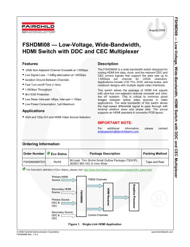
Click here for this datasheet translated into Chinese! FSHDMI08 — Low-Voltage, Wide-Bandwidth, HDMI Switch with DDC and CEC Multiplexer Features Description The FSHDMI08 is a wide-bandwidth switch designed for routing HDMI link data, clock, and the relevant DDC and CEC control signals that support the data rate up to 1.65Gbps per channel for UXGA resolution. Applications include LCD TVs, DVD, set-top boxes, and notebook designs with multiple digital video interfaces. -25db Non-Adjacent Channel Crosstalk at 1.65Gbps Low Signal Loss: -1.5dBg attenuation at 1.65Gbps Isolation Ground Between Channels Fast Turn-on/off Time (< 6ns) 1.65Gbps Throughput This switch allows the passage of HDMI link signals with ultra-low non-adjacent channel crosstalk and ultralow off isolation. This is critical to minimize ghost images between active video sources in video applications. The wide bandwidth of this switch allows the high-speed differential signal to pass through with minimal additive skew and phase jitter. The pinout supports an HDMI standard-A connector PCB layout. 8kV ESD Protection Low Skew: Intra-pair <90ps, Inter-pair < 150ps Low Power Consumption: 1µA Maximum Applications XGA and 720p DVI and HDMI Video Source Selection IMPORTANT NOTE: For additional information, [email protected]. Ordering Information Order Number FSHDMI08MTDX Package Description Packing Method 56-Lead, Thin Shrink Small Outline Package (TSSOP), JEDEC MO-153, 6.1mm Wide For Fairchild’s definition of Eco Status, please visit: http://www.fairchildsemi.com/company/green/rohs_green.html. Primary HDMI Source TMDS Channels Graphics Processor Graphics Processor Graphics Processor HDMI Receiver Secondary HDMI Source Control Channels Figure 1. Single-Link HDMI Application © 2006 Fairchild Semiconductor Corporation FSHDMI08 Rev. 1.0.4 FSHMDI08 — Low-Voltage, Wide-Bandwidth, HDMI Switch with DDC and CEC Multiplexer
Open the catalog to page 1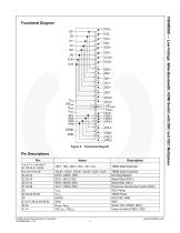
FSHMDI08 — Low-Voltage, Wide-Bandwidth, HDMI Switch with DDC and CEC Multiplexer Figure 2. Functional Diagram TMDS Data Channels TMDS Clock Channels Hot Plug Detects Serial Clock (DDC) Serial Data (DDC) Consumer Electronics Control (CEC) DDC Power TMDS Power DDC/CEC GND GND Select Pins (TMDS, DDC) Output Enable (TMDS, DDC) © 2006 Fairchild Semiconductor Corporation FSHDMI08 Rev. 1.0.4
Open the catalog to page 2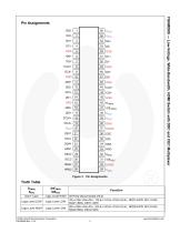
FSHMDI08 — Low-Voltage, Wide-Bandwidth, HDMI Switch with DDC and CEC Multiplexer Truth Table STMDS, SDDC /OETMDS, /OEDDC Don’t’ Care Logic Level HIGH Logic Level HIGH © 2006 Fairchild Semiconductor Corporation FSHDMI08 Rev. 1.0.4
Open the catalog to page 3
Stresses exceeding the absolute maximum ratings may damage the device. The device may not function or be operable above the recommended operating conditions and stressing the parts to these levels is not recommended. In addition, extended exposure to stresses above the recommended operating conditions may affect device reliability. The absolute maximum ratings are stress ratings only. Supply Voltage – TMDS Channels Control Input Voltage STMDS, /OETMDS Control Input Voltage SDDC, /OEDDC Input Clamp Diode Current Switch I/O Current (Continuous) Storage Temperature Range Maximum Junction Temperature...
Open the catalog to page 4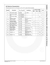
All typical values are for VCC3=3.3V and VDDC=5.0V at 25°C unless otherwise specified. Clamp Diode Voltage Control Input Voltage High Control Input Voltage Low Off State Leakage TMDS Channels Off State Leakage DDC/CEC Channels Control Input Leakage (STMDS, /OETMDS) Control Input Leakage (SDDC, /OEDDC) Quiescent Supply Current -TMDS Quiescent Supply Current -DDC One input at 3.0V; Other inputs at VCC30.6 or VCC3 One input at 3.0V; Other inputs at VDDC © 2006 Fairchild Semiconductor Corporation FSHDMI08 Rev. 1.0.4 FSHMDI08 — Low-Voltage, Wide-Bandwidth, HDMI Switch with DDC and CEC Multiplexer
Open the catalog to page 5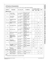
All typical values are for VCC3=3.3V and VDDC=5.0V at 25°C unless otherwise specified. TMDS Channels tONTMDS Turn-On Time S, /OE to Output Turn-Off Time S to Output Switch Propagation (2) Delay Total Jitter (DJ+RJ) Figure 14 f=165MHz clock with 50% duty cycle, RPU=50Ω, CL=5pf Figure 14 Duty Cycle Ratio f=165MHz clock with 50% duty cycle, RPU=50Ω, CL=5pf Intra-Pair Skew (TMDS VCC3=3.0 to 3.6 VDDC =5.0 Cn+ to Cn-) Inter-Pair Skew (Between any two TMDS switch pair paths) VCC3=3.0 to 3.6 Non-Adjacent Channel VDDC =5.0 Crosstalk VCC3=3.0 to 3.6 (TMDS Channels) VDDC =5.0 Off-Isolation (TMDS Channels)...
Open the catalog to page 6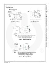
nDm,nCLKm , CECn,HPDn, SCLn, SDAn V CNTRLT = 0 or Vcc3 V CNTRLD = 0 or VDDC V CNTRLT = 0 or Vcc3 V CNTRLD = 0 or VDDC Each switch port is tested separately. RPU and CL are functions of the application environment (see AC/DC tables for values of CL and RPU). CL includes test fixture and stray capacitance. Figure 6. TMDS Test Circuit Load nDm ,nCLKm , CECn,HPDn, SCLn,SDAn VDDC RDDC RPU and CL are functions of the application environment (see AC/DC tables for values of CL and RDDC). CL includes test fixture and stray capacitance. Figure 7. DDC Test Circuit Load © 2006 Fairchild Semiconductor Corporation...
Open the catalog to page 7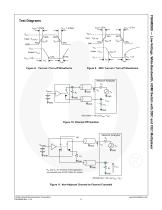
Output - VOUT Input - VCNTRLD Figure 8. Turn-on / Turn-off Waveforms Figure 9. DDC Turn-on / Turn-off Waveforms Network Analyzer RS VCNTRLT Figure 10. Channel Off Isolation R S and R T are functions of the application environment (see AC/DC tables for values). Figure 11. Non-Adjacent Channel-to-Channel Crosstalk © 2006 Fairchild Semiconductor Corporation FSHDMI08 Rev. 1.0.4 FSHMDI08 — Low-Voltage, Wide-Bandwidth, HDMI Switch with DDC and CEC Multiplexer Test Diagrams
Open the catalog to page 8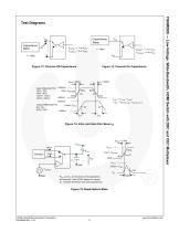
Capacitance Meter Capacitance Meter VCNTRLT = 0 or VCC3 VCNTRLD = 0 or VDDC VCNTRLT = 0 or VCC3 VCNTRLD = 0 or VDDC VSW Figure 12. Channel Off Capacitance Figure 13. Channel On Capacitance tRISE = 240ps Input Differential Pair +500mV Input - VSWTMDS 1Dn+, 1Dn-, 2Dn+, 2Dn-, 1CLK+, 1CLK-, 20% -500mV 2CLK+, 2CLK-, +500mV Output Differential Pair Dn+, Dn-, CLK+, CLK-, Output- VOUT Figure 14. Intra- and Inter-Pair Skew tpd Input - VCNTRLT Output - VOUT R PU and C L are functions of the application environment (see AC/DC tables for values). C L includes test fixture and stray capacitance. Figure 15....
Open the catalog to page 9All Onsemi catalogs and technical brochures
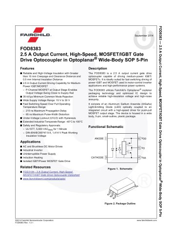
 FOD8383 2.5 A Output Current
18 Pages
 Logic SELECTION GUIDE
12 Pages
 Automotive Solutions Guide
8 Pages
 Motor Drive Solution Guide
20 Pages
 Mobile Solutions Guide
40 Pages
 AUTOMOTIVE SOLUTIONS
16 Pages
 Power Solutions Guide
60 Pages
 STANDARD PRODUCTS GUIDE
72 Pages


Archived catalogs
 Mobile overview
4 Pages
 Analog switch & interface
12 Pages
 TinyLogic® Product Overview
4 Pages
 3:1 Analog Switch Products
2 Pages
 USB Multimedia Switches
2 Pages
 Optocoupler Solutions
24 Pages
 LED LIGHTING SOLUTIONS
16 Pages
 Motor DRIVE solutions
32 Pages
 DIGITAL DISPLAY SOLUTIONS
36 Pages
 RENEWABLE ENERGY SOLUTIONS
32 Pages
 FGPF4536 360V, PDP IGBT
8 Pages
 FSAR001B AC-DC Linear Regulator
12 Pages
 Fairchild - Power solutions
52 Pages















- Position transducer
- Wireless module
- Potentiometer
- Onsemi transistor
- Industrial position sensor
- Motor driver
- Angular position sensor
- Onsemi switching transistor
- Onsemi bipolar transistor
- Digital position sensor
- DC motor motor driver
- Mechanical position sensor
- Signal preamplifier
- DRAM memory module
- Control potentiometer
- CMOS image sensor
- Applications preamplifier
- IGBT transistor
- Onsemi audio transistor
- Inductive position sensor