


FAN5026 Dual-Output/DDR PWM Controller

FAN5026 Dual-Output/DDR PWM Controller
Catalog excerpts
March 2011 © 2005 Fairchild Semiconductor Corporation www.fairchildsemi.com FAN5026 • Rev. 1.0.8 FAN5026 — Dual DDR / Dual-Output PWM Controller FAN5026 Dual DDR / Dual-Output PWM Controller Features Highly Flexible, Dual Synchronous Switching PWM Controller that Includes Modes for: - DDR Mode with In-phase Operation for Reduced Channel Interference - 90° Phase-shifted, Two-stage DDR Mode for Reduced Input Ripple - Dual Independent Regulators, 180° Phase Shifted Complete DDR Memory Power Solution - VTT Tracks VDDQ/2 - VDDQ/2 Buffered Reference Output Lossless Current Sensing on Low-Side MOSFET or Precision Over-Current Using Sense Resistor VCC Under-Voltage Lockout Wide Input Range: 3V to 16V Excellent Dynamic Response with Voltage Feedforward and Average Current-Mode Control Power-Good Signal Supports DDR-II and HSTL 28-Lead Thin-Shrink Small-Outline Package Applications DDR VDDQ and VTT Voltage Generation PC Dual Power Supply Server DDR Power Desktop Computer Graphics Cards Description The FAN5026 PWM controller provides high efficiency and regulation for two output voltages adjustable in the range of 0.9V to 5.5V required to power I/O, chip-sets, and memory banks in high-performance computers, set-top boxes, and VGA cards. Synchronous rectification and hysteretic operation at light loads contribute to high efficiency over a wide range of loads. Efficiency is enhanced by using MOSFET RDS(ON) as a current-sense component. Feedforward ramp modulation, average-current mode control, and internal feedback compensation provide fast response to load transients. Out-of-phase operation with 180-degree phase shift reduces input current ripple. The controller can be transformed into a complete DDR memory power supply solution by activating a designated pin. In DDR Mode, one of the channels tracks the output voltage of another channel and provides output current sink and source capability — essential for proper powering of DDR chips. The buffered reference voltage required by this type of memory is also provided. The FAN5026 monitors these outputs and generates separate PGx (power good) signals when the soft-start is completed and the output is within ±10% of the set point. Over-voltage protection prevents the output voltage from exceeding 120% of the set point. Normal operation is automatically restored when over-voltage conditions cease. Under-voltage protection latches the chip off when output drops below 75% of the set value after the soft-start sequence for this output is completed. An adjustable over-current function monitors the output current by sensing the voltage drop across the lower MOSFET. If precision current-sensing is required, an external current-sense resistor may be used. Related Resources Application Note — AN-6002 Component Calculations and Simulation Tools Ordering Information Part Number Operating Temperature Range Package Packing Method FAN5026MTCX -40 to +85°C 28-Lead Thin-Shrink Small-Outline Package (TSSOP) Tape and Reel
Open the catalog to page 1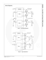
© 2005 Fairchild Semiconductor Corporation www.fairchildsemi.com FAN5026 • Rev. 1.0.8 2 FAN5026 — Dual DDR / Dual-Output PWM Controller Block Diagrams Figure 1. Dual-Output Regulator Figure 2. Typical Application
Open the catalog to page 2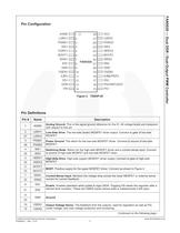
© 2005 Fairchild Semiconductor Corporation www.fairchildsemi.com FAN5026 • Rev. 1.0.8 3 FAN5026 — Dual DDR / Dual-Output PWM Controller Pin Configuration Figure 3. TSSOP-28 Pin Definitions Pin # Name Description 1 AGND Analog Ground. This is the signal ground reference for the IC. All voltage levels are measured with respect to this pin 2 LDRV1 Low-Side Drive. The low-side (lower) MOSFET driver output. Connect to gate of low-side 27 LDRV2 MOSFET. 3 PGND1 Power Ground. The return for the low-side MOSFET driver. Connect to source of low-side 26 PGND2 MOSFET. 4 SW1 Switching Node. Return for the...
Open the catalog to page 3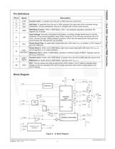
© 2005 Fairchild Semiconductor Corporation www.fairchildsemi.com FAN5026 • Rev. 1.0.8 4 FAN5026 — Dual DDR / Dual-Output PWM Controller Pin Definitions Pin # Name Description 11 ILIM1 Current Limit 1. A resistor from this pin to GND sets the current limit. 12 SS1 Soft Start. A capacitor from this pin to GND programs the slew rate of the converter during initialization. During initialization, this pin is charged with a 5mA 17 SS2 current source. 13 DDR DDR Mode Control. HIGH = DDR Mode. LOW = two separate regulators operating 180 degrees out of phase. 14 VIN Input Voltage. Normally connected to...
Open the catalog to page 4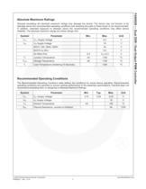
© 2005 Fairchild Semiconductor Corporation www.fairchildsemi.com FAN5026 • Rev. 1.0.8 5 FAN5026 — Dual DDR / Dual-Output PWM Controller Absolute Maximum Ratings Stresses exceeding the absolute maximum ratings may damage the device. The device may not function or be operable above the recommended operating conditions and stressing the parts to these levels is not recommended. In addition, extended exposure to stresses above the recommended operating conditions may affect device reliability. The absolute maximum ratings are stress ratings only. Symbol Parameter Min. Max. Unit VCC VCC Supply Voltage...
Open the catalog to page 5
© 2005 Fairchild Semiconductor Corporation www.fairchildsemi.com FAN5026 • Rev. 1.0.8 6 FAN5026 — Dual DDR / Dual-Output PWM Controller Electrical Characteristics Recommended operating conditions, unless otherwise noted. Symbol Parameter Conditions Min. Typ. Max. Units Power Supplies IVCC VCC Current LDRV, HDRV Open, VSEN Forced Above Regulation Point 2.2 3.0 QA Shutdown (EN-0) 30 QA ISINK VIN Current, Sinking VIN = 15V 10 30 QA ISOURCE VIN Current, Sourcing VIN = 0V -15 -30 QA ISD VIN Current, Shutdown 1 QA VUVLO UVLO Threshold Rising VCC 4.30 4.55 4.75 V Falling 4.10 4.25 4.45 V VUVLOH UVLO...
Open the catalog to page 6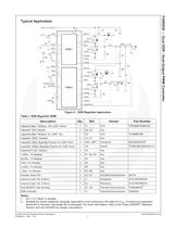
© 2005 Fairchild Semiconductor Corporation www.fairchildsemi.com FAN5026 • Rev. 1.0.8 7 FAN5026 — Dual DDR / Dual-Output PWM Controller Typical Application Figure 5. DDR Regulator Application Table 1. DDR Regulator BOM Description Qty. Ref. Vendor Part Number Capacitor 68Qf, Tantalum, 25V, ESR 150m 1 C1 AVX TPSV686*025#0150 Capacitor 10nf, Ceramic 2 C2, C3 Any Capacitor 68Qf, Tantalum, 6V, ESR 1.8 1 C4 AVX TAJB686*006 Capacitor 150nF, Ceramic 2 C5, C7 Any Capacitor 180Qf, Specialty Polymer 4V, ESR 15m 2 C6A, C6B(1) Panasonic EEFUE0G181R Capacitor 1000Qf, Specialty Polymer 4V, ESR 10m 1 C8 Kemet...
Open the catalog to page 7All Onsemi catalogs and technical brochures
 FOD8383 2.5 A Output Current
18 Pages
 Logic SELECTION GUIDE
12 Pages
 Automotive Solutions Guide
8 Pages
 Motor Drive Solution Guide
20 Pages
 Mobile Solutions Guide
40 Pages
 AUTOMOTIVE SOLUTIONS
16 Pages
 Power Solutions Guide
60 Pages
 STANDARD PRODUCTS GUIDE
72 Pages


Archived catalogs
 Mobile overview
4 Pages
 Analog switch & interface
12 Pages
 TinyLogic® Product Overview
4 Pages
 3:1 Analog Switch Products
2 Pages
 USB Multimedia Switches
2 Pages
 Optocoupler Solutions
24 Pages
 LED LIGHTING SOLUTIONS
16 Pages
 Motor DRIVE solutions
32 Pages
 DIGITAL DISPLAY SOLUTIONS
36 Pages
 RENEWABLE ENERGY SOLUTIONS
32 Pages
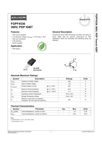 FGPF4536 360V, PDP IGBT
8 Pages
 FSAR001B AC-DC Linear Regulator
12 Pages
 Fairchild - Power solutions
52 Pages















- Position transducer
- Wireless module
- Potentiometer
- Onsemi transistor
- Industrial position sensor
- Motor driver
- Angular position sensor
- Onsemi switching transistor
- Onsemi bipolar transistor
- Digital position sensor
- DC motor motor driver
- Mechanical position sensor
- Signal preamplifier
- DRAM memory module
- Control potentiometer
- CMOS image sensor
- Applications preamplifier
- IGBT transistor
- Onsemi audio transistor
- Inductive position sensor