Catalog excerpts

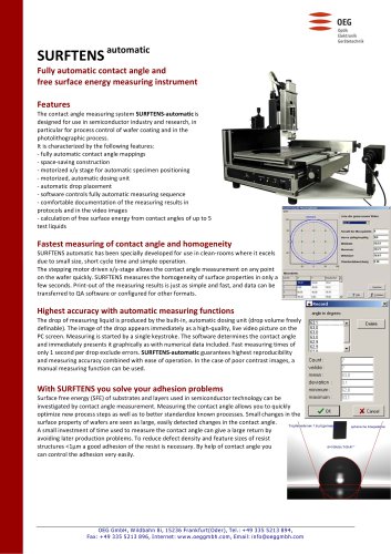
Fully automatic contact angle and free surface energy measuring instrument Features The contact angle measuring system SURFTENS‐automatic is designed for use in semiconductor industry and research, in particular for process control of wafer coating and in the photolithographic process. It is characterized by the following features: ‐ fully automatic contact angle mappings ‐ space‐saving construction ‐ motorized x/y stage for automatic specimen positioning ‐ motorized, automatic dosing unit ‐ automatic drop placement ‐ software controls fully automatic measuring sequence ‐ comfortable documentation of the measuring results in protocols and in the video images ‐ calculation of free surface energy from contact angles of up to 5 test liquids Fastest measuring of contact angle and homogeneity SURFTENS automatic has been specially developed for use in clean‐rooms where it excels due to small size, short cycle time and simple operation. The stepping motor driven x/y‐stage allows the contact angle measurement on any point on the wafer quickly. SURFTENS measures the homogeneity of surface properties in only a few seconds. Print‐out of the measuring results is just as simple and fast, and data can be transferred to QA software or configured for other formats. Highest accuracy with automatic measuring functions The drop of measuring liquid is produced by the built‐in, automatic dosing unit (drop volume freely definable). The image of the drop appears immediately as a high‐quality, live video picture on the PC screen. Measuring is started by a single keystroke. The software determines the contact angle and immediately presents it graphically as with numerical data included. Fast measuring times of only 1 second per drop exclude errors. SURFTENS‐automatic guarantees highest reproducibility and measuring accuracy combined with ease of operation. In the case of poor contrast images, a manual measuring function can be used. With SURFTENS you solve your adhesion problems Surface free energy (SFE) of substrates and layers used in semiconductor technology can be investigated by contact angle measurement. Measuring the contact angle allows you to quickly optimize new process steps as well as to better standardize known processes. Small changes in the surface property of wafers are seen as large, easily detected changes in the contact angle. A small investment of time used to measure the contact a
Open the catalog to page 1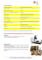
Technical parameters Specimen table (standard) Specimen thickness Measuring range contact angle Resolution / accuracy contact angle measurement Optics (standard) drop placement Camera (standard) Tilt of measuring optics Dosing unit (standard) Reproducibility of drop volume Software Light source Computer SURFTENS HL SURFTENS HL is a manual contact angle measuring system for Si‐Wafers. It can be equipped with a motorized dosing unit.
Open the catalog to page 2All OEG catalogs and technical brochures
-
RTM
2 Pages
-
ELCOWIN & ELCOLEVEL
2 Pages
-
GPM2
2 Pages
-
Flatscan 650 3D
7 Pages
-
SURFTENS‐Basic
2 Pages
-
OPTICAL HEIGHT GAUGE OHM 150
2 Pages
-
MTF Master 200
2 Pages

