


ST7735P3
ST7735P3
Catalog excerpts
Sitronix Technology Corporation Sitronix Technology Corp. reserves the right to change the contents in this document without prior notice.
Open the catalog to page 1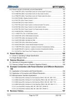
13 Example Connection with Panel Direction and Different Resolution 190
Open the catalog to page 6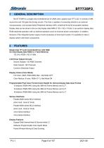
GENERAL DESCRIPTION The ST7735P3 is a single-chip controller/driver for 262K-color, graphic type TFT-LCD. It consists of 396 source line and 162 gate line driving circuits. This chip is capable of connecting directly to an external microprocessor, and accepts Serial Peripheral Interface (SPI), 8-bit/9-bit/16-bit/18-bit parallel interface. Display data can be stored in the on-chip display data RAM of 132 x 162 x 18 bits. It can perform display data RAM read/write operation with no external operation clock to minimize power consumption. In addition, because of the integrated power supply circuits...
Open the catalog to page 9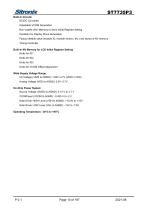
ST7735P3 Built-in Circuits DC/DC Converter Adjustable VCOM Generation Non-volatile (NV) Memory to Store Initial Register Setting Oscillator for Display Clock Generation Factory default value (module ID, module version, etc.) are stored in NV memory. Timing Controller Built-in NV Memory for LCD Initial Register Setting 8-bits for ID1 8-bits for ID2 8-bits for ID3 5-bits for VCOM Offset Adjustment Wide Supply Voltage Range I/O Voltage (VDDI to DGND): 1.65V~3.7V (VDDI ≤ VDD) Analog Voltage (VDD to AGND): 2.5V~3.7V On-Chip Power System Source Voltage (GVDD to AGND): 3.15 V to 4.7 V VCOM level (VCOM...
Open the catalog to page 10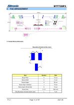
View Point Input Pad Input Pad(interface) 3.1 Output Bump Dimension Boundary (Include scribe Lane) Bump Pitch Bump Width Bump Height Bump Area Chip Boundary (Include Scribe Lane)
Open the catalog to page 11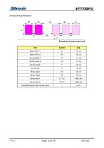
3.2 Input Bump Dimension Boundary (Include scribe Lane)
Open the catalog to page 12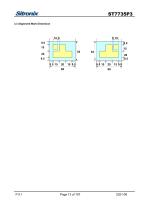
ST7735P3 3.3 Alignment Mark Dimension
Open the catalog to page 13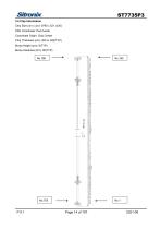
ST7735P3 3.4 Chip Information Chip Size (um x um): 9795 x 521 (±30) PAD Coordinate: Pad Center Coordinate Origin: Chip Center Chip Thickness (um): 200 or 300(TYP) Bump Height (um): 9(TYP) Bump Hardness (HV): 90(TYP) No.186 DUMMY VCOM VCOM VCOM VCL VCL VCL DUMMY DUMMY DUMMY DUMMY DUMMY VGH VGL VGL VGL DUMMY DUMMY DUMMY DUMMY DUMMY DUMMY DUMMY DUMMY DUMMY DUMMY DUMMY DUMMY DUMMY DUMMY DUMMY DUMMY DUMMY DUMMY AVCL AVCL AVCL AGND AGND AGND DUMMY DUMMY DUMMY DUMMY DUMMY DUMMY DUMMY DUMMY DUMMY DUMMY DUMMY DUMMY DUMMY DUMMY DUMMY DUMMY DUMMYR DUMMYR DUMMY DUMMY DUMMY AVDD AVDD AVDD AVDD AVDD DUMMY...
Open the catalog to page 14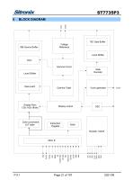
Level Shifter Gamma Circuit Level Shifter Data Latch Gamma Table Vcom generator Display control
Open the catalog to page 21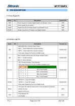
-8080/6800 MCU Interface Mode Select. -P68=’1’, Select 6800 MCU Parallel Interface. -P68=’0’, Select 8080 MCU Parallel Interface. -If not used, Please Fix this Pin at DGND Level. MCU Parallel Interface Bus and Serial Interface select I IM2=’ 1 Parallel Interface IM2=’0’, Serial Interface - MCU Parallel Interface Type Selection -If Not Used, Please Fix this Pin at VDDI or DGND Level. -If Not Used, Please fix this Pin at DGND Level. -This signal will reset the device and it must be applied to properly initialize the chip. -Chip Selection Pin -Low Enable.
Open the catalog to page 22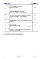
Notel. When in parallel mode, no use data pin must be connected to “1” or “0”. Note2. When CSX=”1”, there is no influence to the parallel and serial interface.
Open the catalog to page 23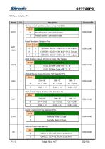
Description Connect Pin EXTC - During normal operation, please connect to VDDI..
Open the catalog to page 24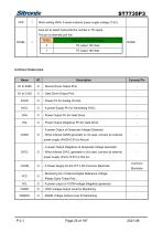
I When writing NVM, it needs external power supply voltage (7.5V). Input pin to select horizontal line number in TE signal. This pin is internally pull low.
Open the catalog to page 25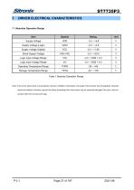
7.1 Absolute Operation Range Table 1 Absolute Operation Range Note: If one of the above items is exceeded its maximum limitation momentarily, the quality of the product may be degraded. Absolute maximum limitation, therefore, specify the values exceeding which the product may be physically damaged. Be sure to use the product within the recommend range.
Open the catalog to page 27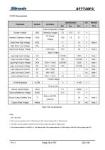
2. Source channel loading= 2KQ+12pF/channel, Gate channel loading=5KH+40pF/channel. 3. The Max. value is between measured point of source output and gamma setting value. 4. VGH setting condition is A VDD=4.7 V, the Max and Min VGH voltage depend on AVDD setting, VGH-VGL can not large than 30 V.
Open the catalog to page 28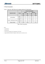
Table 3 Power Consumption 3. The Current Consumption is DC characteristics of ST7735P3
Open the catalog to page 29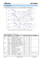
ST7735P3 8 Timing chart 8.1 Parallel Interface Characteristics: 18, 16, 9 or 8-bit Bus (8080 Series MCU Interface) TCHW TRC/TRCFM TRDL/TRDLFM Figure 1 Parallel Interface Timing Characteristics (8080 Ceries MCU Interface) Address Setup Time Address Hold Time (Write/Read) Chip Select “H” Pulse Width Chip Select Setup Time (Write) Chip Select Setup Time (Read ID) Chip Select Setup time (Read FM) Chip Select Wait Time (Write/Read) Chip Select Hold Time Write Cycle Control Pulse “H” Duration Control Pulse “L” Duration Control Pulse “H” Duration (ID) Control Pulse “L” Duration (ID)
Open the catalog to page 30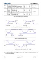
Table 4 8080 Parallel Interface Characteristics Note: The rising time and falling time (Tr, Tf) of input signal are specified at 15 ns or less. Logic high and low levels are specified as 30% and 70% of VDDI for Input signals.
Open the catalog to page 31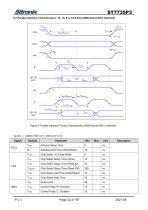
ST7735P3 8.2 Parallel Interface Characteristics: 18, 16, 9 or 8-bit Bus (6800 Series MCU Interface) Figure 5 Parallel Interface Timing Characteristics (6800-Series MCU Interface) Address Setup Time Address Hold Time (Write/Read) Chip Select “H” Pulse Width Chip Select Setup Time (Write) Chip Select Setup Time (Read ID) Chip Select Setup Time (Read FM) Chip Select wait Time (Write/Read) Chip Select Hold Time Write Cycle Control Pulse “H” Duration Control Pulse “L” Duration
Open the catalog to page 32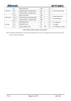
Table 5 6800 Parallel Interface Characteristics Note: The rising time and falling time (Tr, Tf) of input signal are specified at 15 ns or less. Logic high and low levels are specified as 30% and 70% of VDDI for Input signals
Open the catalog to page 33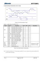
ST7735P3 8.3 Serial Interface Characteristics (3-line Serial) TCSS TSLW/TSLR TSHW/TSHR TSDS Figure 6 3-line Serial Interface Timing Ta=25 ℃, VDDI=1.65~3.7V, VDD=2.5~3.7V Signal Chip Select Setup Time (Write) Chip Select Hold Time (Write) Chip Select Setup Time (Read) Chip Select Hold Time (Read) Chip Select “H” pulse width Serial Clock Cycle (Write) SCL “H” Pulse Width (Write) SCL “L” Pulse Width (Write) Serial Clock Cycle (Read) SCL “H” Pulse Width (Read) SCL “L” Pulse Width (Read) Data Setup Time Data Hold Time Access Time Output Disable Time Table 6 3-line Serial Interface Characteristics...
Open the catalog to page 34All NEWHAVEN DISPLAY INTERNATIONAL catalogs and technical brochures
 FT5426G
19 Pages
 FT5336GQQ
13 Pages
 FT5x16
15 Pages
 PT6324
5 Pages
 PT6321
6 Pages
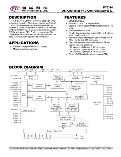 PT6314
42 Pages
 PT6302
43 Pages
 HT16528
40 Pages
 ILI9341V
249 Pages
 ST7735S
201 Pages
 EK79202D
78 Pages
 LT6911C
21 Pages
 SSD1306
59 Pages
 SSD1305
70 Pages
 SEPS525
46 Pages
 SEPS114
43 Pages
 SSD1333
36 Pages
 SSD1353
75 Pages
 IST3602
64 Pages
 SSD1333
36 Pages
 SSD1353
75 Pages