


SSD1353
SSD1353
Catalog excerpts
SOLOMON SYSTECH SEMICONDUCTOR TECHNICAL DATA This document contains information on a new product. Specifications and information herein are subject to change without notice. Copyright © 2008 Solomon Systech Limited SVSTECH
Open the catalog to page 1
Solomon Systech
Open the catalog to page 2
Solomon Systech
Open the catalog to page 4
Solomon Systech
Open the catalog to page 5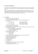
GENERAL DESCRIPTION The SSD1353 is a CMOS OLED/PLED driver with 480 segments and 132 commons output, supporting up to 160RGB x 132 dot matrix display. This chip is designed for Common Cathode type OLED/PLED panel. The SSD1353 had embedded Graphic Display Data RAM (GDDRAM). It supports with 8, 9, 16, 18 bits 8080 / 6800 parallel interface as well as Serial Peripheral Interface. It has 256-step contrast and 262K color control, giving vivid color display to OLED panels. This driver IC can be widely used in many applications such as MP3, PDA, PMP, mobile phone and Digital Camera. Resolution: 160...
Open the catalog to page 6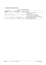
Table 3-1 : Ordering Information Solomon Systech
Open the catalog to page 7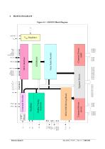
Figure 4-1 : SSD1353 Block Diagram VSYNC ■ HSYNC • DOTCLK • PDEN • Solomon Systech
Open the catalog to page 8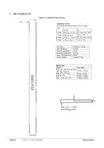
Alignment marks (For details dimension please refer to Figure 5-2) _._ Bump Size Solomon Systech
Open the catalog to page 9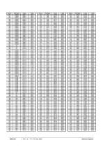
Solomon Systech
Open the catalog to page 11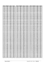
Solomon Systech
Open the catalog to page 12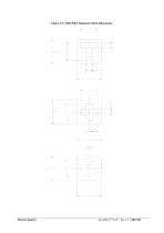
Figure 5-2: SSD1335Z Alignment Mark Dimensions Solomon Systech
Open the catalog to page 14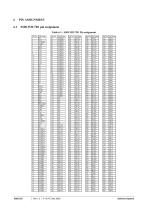
Solomon Systech
Open the catalog to page 15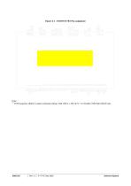
Note:(1) COM sequence (Split) is under command setting: A0h, 60h (i.e. Bit A[5] =1 to Enable COM Split Odd Even) . Solomon Systech
Open the catalog to page 17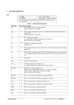
Solomon Systech
Open the catalog to page 18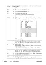
Pin Type Description Vbref This is an internal voltage reference pin. A capacitor should be connected to this pin and Vss. This is a reserved pin. It should be kept NC. This is a reserved pin. It should be kept NC. This is segment voltage reference pin. When external VSL is not used, this pin should be left open. When external VSL is used, connect with resistor and diode to ground. (details depend on application) MCU bus interface selection pins. Select appropriate logic setting as described in the following table. Table 7-2 : Bus Interface selection This pin is the segment output current reference...
Open the catalog to page 19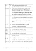
Solomon Systech
Open the catalog to page 20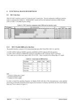
SSD1353 MCU interface consist of 18 data pin and 5 control pins. The pin assignment at different interface mode is summarized in Table 8-1. Different MCU mode can be set by hardware selection on BS[3:0] pins (refer to Table 7-2 for BS[3:0] pins setting) Table 8-1 : MCU interface assignment under different bus interface mode (1) i stands for falling edge of signal (2) H stands for HIGH in signal In order to match the operating frequency of display RAM with that of the microprocessor, some pipeline processing is internally performed which requires the insertion of a dummy read before the first...
Open the catalog to page 21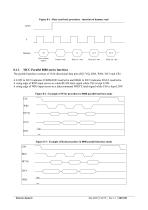
Figure 8-1 : Data read back procedure - insertion of dummy read R/W# Write column address Dummy read The parallel interface consists of 18 bi-directional data pins (D[17:0]), RD#, WR#, D/C# and CS#. A LOW in D/C# indicates COMMAND read/write and HIGH in D/C# indicates DATA read/write. A rising edge of RD# input serves as a data READ latch signal while CS# is kept LOW. A rising edge of WR# input serves as a data/command WRITE latch signal while CS# is kept LOW. Figure 8-2 : Example of Write procedure in 8080 parallel interface mode CS# WR# D[7:0] Figure 8-3 : Example of Read procedure in 8080...
Open the catalog to page 22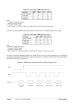
Table 8-3 : Control pins of 8080 interface (Form 1) (1) t stands for rising edge of signal (2) H stands for HIGH in signal (4) Refer to Figure 13-3 for Form 2 8080-Series MPU Parallel Interface Timing Characteristics In order to match the operating frequency of display RAM with that of the microprocessor, some pipeline processing is internally performed which requires the insertion of a dummy read before the first actual display data read. This is shown in Figure 8-4. Figure 8-4 : Display data read back procedure - insertion of dummy read Dummy read Read 1st data Read 2nd data Solomon Systech
Open the catalog to page 23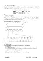
8.1.3 MCU Serial Interface The serial interface consists of serial clock SCLK, serial data SDIN, D/C#, CS#. In SPI mode, DO acts as SCLK, D1 acts as SDIN. For the unused data pins, D2 should be left open. The pins from D3 to D17, E and R/W# can be connected to an external ground. Table 8-5 : Control pins of Serial interface (1) H stands for HIGH in signal SDIN is shifted into an 8-bit shift register on every rising edge of SCLK in the order of D7, D6, ... D0. D/C# is sampled on every eighth clock and the data byte in the shift register is written to the Graphic Display Data RAM (GDDRAM) or command...
Open the catalog to page 24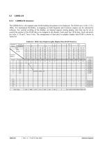
The GDDRAM is a bit mapped static RAM holding the pattern to be displayed. The RAM size is 160 x 132 x 18bits. For mechanical flexibility, re-mapping on both Segment and Common outputs can be selected by software. For vertical scrolling of the display, an internal register storing display start line can be set to control the portion of the RAM data to be mapped to the display. Each pixel has 18-bit data. Each sub-pixels for color A, B and C have 6 bits. The arrangement of data pixel in graphic display data RAM is shown in Table 8-6 Table 8-6 : 262k Color Depth Graphic Display Data RAM Structure...
Open the catalog to page 25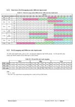
Table 8-7 : Data bus usage under different bus width and color depth mode Solomon Systech
Open the catalog to page 26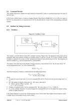
Command Decoder This module determines whether the input should be interpreted as data or command based upon the input of the D/C# pin. If D/C# pin is HIGH, data is written to Graphic Display Data RAM (GDDRAM). If it is LOW, the inputs at D0-D17 are interpreted as a Command and it will be decoded and be written to the corresponding command register. Oscillator & Timing Generator Oscillator Figure 8-6 : Oscillator Circuit Internal Oscillator Fosc M U X DCLK Display Clock This module is an On-Chip low power RC oscillator circuitry (Figure 8-6). The operation clock (CLK) can be generated either...
Open the catalog to page 27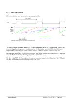
FR synchronization signal can be used to prevent tearing effect. One frame 100% Memory Access Process 0% Time Fast write MCU Slow write MCU SSD1353 displaying memory updates to OLED screen The starting time to write a new image to OLED driver is depended on the MCU writing speed. If MCU can finish writing a frame image within one frame period, it is classified as fast write MCU. For MCU needs longer writing time to complete ( more than one frame but within two frames), it is a slow write one. For fast write MCU: MCU should start to write new frame of ram data just after rising edge of FR pulse...
Open the catalog to page 28All NEWHAVEN DISPLAY INTERNATIONAL catalogs and technical brochures
 FT5426G
19 Pages
 FT5336GQQ
13 Pages
 FT5x16
15 Pages
 PT6324
5 Pages
 PT6321
6 Pages
 PT6314
42 Pages
 PT6302
43 Pages
 HT16528
40 Pages
 ILI9341V
249 Pages
 ST7735S
201 Pages
 ST7735P3
197 Pages
 EK79202D
78 Pages
 LT6911C
21 Pages
 SSD1306
59 Pages
 SSD1305
70 Pages
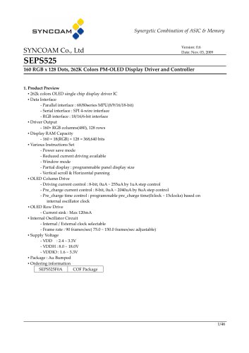 SEPS525
46 Pages
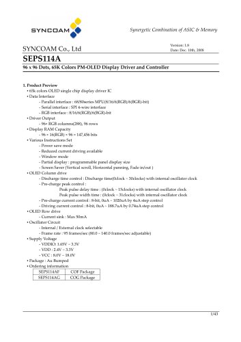 SEPS114
43 Pages
 SSD1333
36 Pages
 IST3602
64 Pages
 SSD1333
36 Pages
 SSD1353
75 Pages