


SSD1333
SSD1333
Catalog excerpts
SOLOMON SYSTECH SEMICONDUCTOR TECHNICAL DATA This document contains information on a new product. Specifications and information herein are subject to change without notice. Copyright © 2018 Solomon Systech Limited SYSTECH
Open the catalog to page 1
Appendix: IC Revision history of SSD1333 Specification Solomon Systech
Open the catalog to page 2
Solomon Systech
Open the catalog to page 4
Solomon Systech
Open the catalog to page 5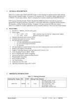
SSD1333 is a single-chip CMOS OLED/PLED driver with controller for organic/polymer light emitting diode dot-matrix graphic display. It consists of 528 segments and 176 commons output, supporting up to 176RGB x 176 dot matrix display. This IC is designed for Common Cathode type OLED/PLED panel. SSD1333 has embedded Graphic Display Data RAM (GDDRAM). Data/Commands are sent from general MCU through the hardware selectable 8, 16 bits 6800-/8080-series compatible Parallel Interface, I2C Interface, or Serial Peripheral Interface. It supports 256-step contrast and 65K color control. SSD1333 is suitable...
Open the catalog to page 6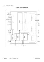
BLOCK DIAGRAM Figure 4-1 –SSD1333 Block Diagram Common Drivers Gray Scale Decoder Segment Drivers Common Drivers SEG/COM Driving Block Display Timing Generator Command Decoder Solomon Systech
Open the catalog to page 7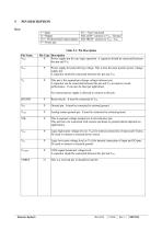
Solomon Systech
Open the catalog to page 8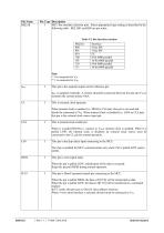
MCU bus interface selection pins. Select appropriate logic setting as described in the following table. BS2, BS1 and BS0 are pin select. Table 5-2: Bus Interface selection I This pin is the segment output current reference pin. IREF is supplied externally. A resistor should be connected between this pin and VSS to maintain the current around 10uA. I This is external clock input pin. When internal clock is enabled (i.e. HIGH in CLS pin), this pin is not used and should be connected to Vss. When internal clock is disabled (i.e. LOW in CLS pin), this pin is the external clock source input pin. I...
Open the catalog to page 9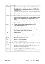
Solomon Systech
Open the catalog to page 10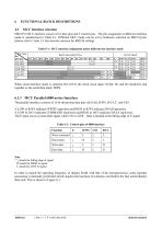
SSD1333 MCU interface consist of 16 data pins and 5 control pins. The pin assignment at different interface mode is summarized in Table 6-1. Different MCU mode can be set by hardware selection on BS[2:0] pins (please refer to Table 5-2: Bus Interface selection for BS[2:0] setting). Table 6-1 : MCU interface assignment under different bus interface mode (1) i stands for falling edge of signal H stands for HIGH in signal L stands for LOW in signal In order to match the operating frequency of display RAM with that of the microprocessor, some pipeline processing is internally performed which requires...
Open the catalog to page 11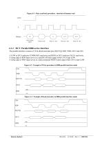
Figure 6-1 : Data read back procedure - insertion of dummy read R/W# Write column address Dummy read 6.1.2 MCU Parallel 8080-series Interface The parallel interface consists of 16 bi-directional data pins (D[15:0]), RD#, WR#, D/C# and CS#. A LOW in D/C# indicates COMMAND read/write and HIGH in D/C# indicates DATA read/write. A rising edge of RD# input serves as a data READ latch signal while CS# is kept LOW. A rising edge of WR# input serves as a data/command WRITE latch signal while CS# is kept LOW. Figure 6-2 : Example of Write procedure in 8080 parallel interface mode CS# WR# D[15:0] Figure...
Open the catalog to page 12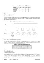
Table 6-3 : Control pins of 8080 interface (1) H stands for HIGH in signal (3) T stands for rising edge of signal SDIN is shifted into an 8-bit shift register on every rising edge of SCLK in the order of D7, D6, ... D0. D/C# is sampled on every eight clocks and the data byte in the shift register is written to the Graphic Display Data RAM (GDDRAM) or command register in the same clock. D/C# should keep its stage from the start to the end of operation. Solomon Systech
Open the catalog to page 13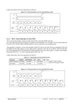
Under serial mode, only write operations are allowed. Figure 6-5 : Write procedure in 4-wire Serial interface mode -^iX^DCDiX!D!X!DiX!D2XiiXDC>—6.1.4 MCU Serial Interface (3-wire SPI) The 3-wire serial interface consists of serial clock SCLK, serial data SDIN and CS#. In 3 -wire SPI mode, DO acts as SCLK, D1 and D2 are tied together to act as SDIN. For the unused data pins from D3 to D15, R/W# (WR#), E(RD#) and D/C# can be connected to an external ground. The operation is similar to 4-wire serial interface while D/C# pin is not used. There are altogether 9-bits will be shifted into the shift...
Open the catalog to page 14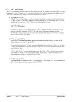
The I2C communication interface consists of slave address bit SA0, I2C-bus data signal SDA (SDAOUT/D2 for output and SDAIN/D1 for input) and I2C-bus clock signal SCL (D0). Both the data and clock signals must be connected to pull-up resistors. RES# is used for the initialization of device. a) Slave address bit (SA0) SSD1333 has to recognize the slave address before transmitting or receiving any information by the I2C-bus. The device will respond to the slave address following by the slave address bit (“SA0” bit) and the read/write select bit (“R/W#” bit) with the following byte format, b7 b6...
Open the catalog to page 15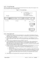
6.1.5.1 I2C-bus Write data The I2C-bus interface gives access to write data and command into the device. Please refer to Figure 6-7 for the write mode of I2C-bus in chronological order. Figure 6-7 : I2C-bus data format D/C# - Data / Command Selection bit R/W# - Read / Write Selection bit Write mode S - Start Condition / P - Stop Condition Slave Address Control byte Data byte 6.1.5.2 Write mode for I2C 1) The master device initiates the data communication by a start condition. The definition of the start condition is shown in Figure 6-8. The start condition is established by pulling the SDA from...
Open the catalog to page 16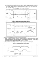
7) The write mode will be finished when a stop condition is applied. The stop condition is also defined in Figure 6-8. The stop condition is established by pulling the “SDA in” from LOW to HIGH while the “SCL” stays HIGH. Figure 6-8 : Definition of the Start and Stop Condition tHSTART tSSTOP START START condition STOP condition Figure 6-9 : Definition of the acknowledgement condition DATA OUTPUT BY TRANSMITTER Non-acknowledge DATA OUTPUT BY RECEIVER Acknowledge SCL FROM MASTER Clock pulse for acknowledgement START Condition Please be noted that the transmission of the data bit has some limitations....
Open the catalog to page 17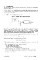
Command Decoder This module determines whether the input data is interpreted as data or command. Data is interpreted based upon the input of the D/C# pin. If D/C# pin is HIGH, D[7:0] is interpreted as display data written to Graphic Display Data RAM (GDDRAM). If it is LOW, the input at D[7:0] is interpreted as a command. Then data input will be decoded and written to the corresponding command register. Oscillator Circuit and Display Time Generator Figure 6-11 : Oscillator Circuit and Display Time Generator Internal Oscillator Fosc M U X Display Clock This module is an on-chip LOW power RC oscillator...
Open the catalog to page 18All NEWHAVEN DISPLAY INTERNATIONAL catalogs and technical brochures
 FT5426G
19 Pages
 FT5336GQQ
13 Pages
 FT5x16
15 Pages
 PT6324
5 Pages
 PT6321
6 Pages
 PT6314
42 Pages
 PT6302
43 Pages
 HT16528
40 Pages
 ILI9341V
249 Pages
 ST7735S
201 Pages
 ST7735P3
197 Pages
 EK79202D
78 Pages
 LT6911C
21 Pages
 SSD1306
59 Pages
 SSD1305
70 Pages
 SEPS525
46 Pages
 SEPS114
43 Pages
 SSD1333
36 Pages
 SSD1353
75 Pages
 IST3602
64 Pages
 SSD1353
75 Pages