SEPS525
1 /46Pages
SEPS525
1 /46Pages
Catalog excerpts
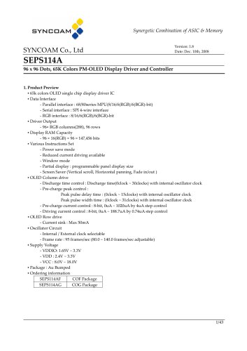
Synergetic Combination of ASIC & Memory ■ 262k colors OLED single chip display driver IC - Serial interface : SPI 4-wire interface - Power save mode - Reduced current driving available - Window mode - Partial display : programmable panel display size - Vertical scroll & Horizontal panning ■ OLED Column Drive - Driving current control : 8-bit, 0uA ~ 255uA by 1uA step control - Pre_charge current control : 8-bit, 0uA ~ 2040uA by 8uA step control - Pre_charge time control : programmable pre_charge time(0clock ~ 15clocks) based on internal oscillator clock ■ Internal Oscillator Circuit - Internal / External clock selectable - Frame rate : 90 frames/sec( 75.0 ~ 150.0 frames/sec adjustable) - VDDIO : 1.6 ~ 3.3V 1 Package : Au Bumped
Open the catalog to page 1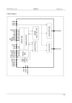
VSDH VSSH VDDH 480 Column Driver 128 Row Driver OSCA1 OSCA2 VDDH VSSH VSDH Timing Controller VDDIO VDD VSS ENABLE HSYNC VSYNC DOTCLK VSYNCO Instruction Registers RESETB CPU PS CSB RS RDB/E WRB/RWB DB[17:0]
Open the catalog to page 2
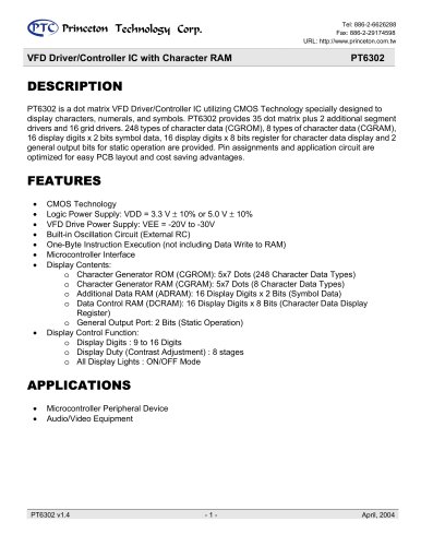
4. Functional Description MPU Interface The SEPS525 has three high-speed system interface : a 68-system, an 80-system 8/9/16/18 bit bus, and a clock synchronous serial(SPI : Serial Peripheral Interface). Among the interface modes, a specific mode is selected by the setting of PS pin and MEMORY_WRITE_MODE register(16h). The SEPS525 has 3-type registers : an index register(IR) 8-bits, a write data register(WDR), and a read data register(RDR). The IR stores index information for the control registers and the DDRAM. The WDR temporarily stores data to be written into control registers and the DDRAM,...
Open the catalog to page 4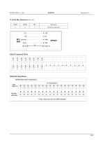
1 Pixel : 262k color with 18-bit MPU interface
Open the catalog to page 5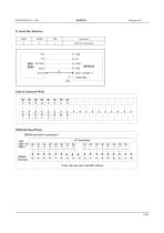
DDRAM Read/Write DDRAM data write(1-transmission) Input DB[17:10] DB[8:1] DDRAM write data 1 Pixel : 65k color with 16-bit MPU interface
Open the catalog to page 6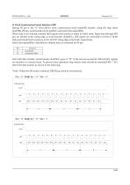
5) Clock Synchronized Serial Interface (SPI) Setting PS pin to the "0" level allows clock synchronized serial data(SPI) transfer, using the chip select pin(CSB), RS pin, serial transfer clock pin(SCL) and serial data input(SDI). When chip is not selected, internal shift register and counter is resets to initial value. Input data through SDI pin are latched at the rising edge of serial transfer clock(SCL). SDI inputs are converted to 16-bit or 18-bit data and transferred to memory at the 16th/18th rising edge serial clock, respectively. Serial data input(SDI) is identified to display data or command...
Open the catalog to page 9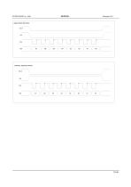
INDEX REGISTER WRITE CONTROL REGISTER WRITE
Open the catalog to page 10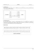
6) RGB Interface When the RGB_IF register bit0 is set to “0”, SEPS525 enters into the RGB interface mode and DDRAM write cycle is synchronized by DOTCLK. 18-bit RGB interface The 18-bit RGB interface is selected by setting RIM[1:0] bits to “00”. DDRAM write operation is Synchronized with DOTCLK and ENABLE. Display data are transmitted to DDRAM in synchronization with 18-bit RGB data bus(DB[17:0]) and the data enable(ENABLE). DDRAM Write Data format for 18-bit RGB interface
Open the catalog to page 11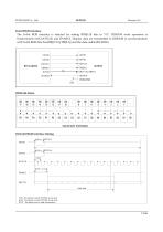
16-bit RGB interface The 16-bit RGB interface is selected by setting RIM[1:0] bits to “01”. DDRAM write operation is Synchronized with DOTCLK and ENABLE. Display data are transmitted to DDRAM in synchronization with 16-bit RGB data bus(DB[17:10], DB[8:1]) and the data enable(ENABLE). Data format for 16-bit interface 18/16-bit RGB interface timing V LW >= 1D O TC LK VSYNC V LW : the period in w hich V S Y N C is low level H LW : the period in w hich H S Y N C is low level D T S T : the setup tim e for data transm ission
Open the catalog to page 12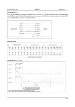
The 6-bit RGB interface is selected by setting RIM[1:0] bits to "10". DDRAM write operation is Synchronized with DOTCLK and ENABLE. Display data are transmitted to DDRAM in synchronization with 6-bit RGB data bus(DB[17:12]) and the data enable(ENABLE). Data format for 6-bit interface
Open the catalog to page 13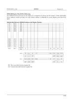
The DDRAM stores pixel data for the display. It is composed of 128-row by 160-column x 18-bit addressable array. Address counter provides row and column address to DDRAM for access display pixel data from RD : Row scan shift direction register bit. CD : Column data shift direction register bit.
Open the catalog to page 14
Window Address Function When data is written to the on-chip DDRAM, a window address-range which is specified by the horizontal address register(start : MX1[7:0], end : MX2[7:0]) or the vertical address register(start : MY1[7:0], end : MY2[7:0]) can be written to consecutively. Data is written to addresses in the direction specified by the HC, VC(increment/decrement), and HV bit(H or V direction). When the image data is being written, data can be written consecutively without thinking of a data wrap by doing this. The window must be specified within the DDRAM address area described below, Addresses...
Open the catalog to page 15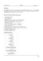
Reset Status The SEPS525 is initialized as following description when RESETB terminal is set to “L”. Usually RESETB terminal is connected reset terminal of MPU, so that the chip can be initialized simultaneously with MPU. The SEPS525 should be initialized when the power is on. INITIAL SETTING CONDITION (default setting) 1. Frame frequency : 90Hz 2. OSC : internal OSC 3. Internal OSC : ON 4. DDRAM write horizontal address : MX1 = 00h, MX2 = 9Fh 5. DDRAM write vertical address : MY1 = 00h, MY2 = 7Fh 6. Display data RAM write : HC = 1, VC = 1, HV = 0 7. RGB data swap : OFF 8. Row scan shift direction...
Open the catalog to page 16
IREF : Control reference voltage generation.When IREF = 0, Reference voltage controlled by external resister When IREF = 1, Reference voltage controlled by internal resisterCLOCK_DIV (03h) DFR[3:0] : Display frequency divide ration DFR3
Open the catalog to page 19
PREM : Precharge mode select. When PREM = 0, Scan signal is high level at pre_charge period When PREM = 1, Scan signal is low level at pre_charge period DON : Display ON/OFF. When DON = 0, Turns the display off When DON = 1, Turns the display on
Open the catalog to page 20
DCR[7:0] : DCR driving current R. DCG[7:0] : DCG driving current G. DCB[7:0] : DCB driving current B. * Driving current = setting value * 1uA.
Open the catalog to page 22
VSYOEN : Vsync. Output enable(0 : VSYNCO disable). DOP : Dot clock polarity(0 : sampled at rising edge). ENP : Enable polarity(0 : active low). Note) All reserved signals(RES) must write to '0'.
Open the catalog to page 24All NEWHAVEN DISPLAY INTERNATIONAL catalogs and technical brochures
 FT5426G
19 Pages
 FT5336GQQ
13 Pages
 FT5x16
15 Pages
 PT6324
5 Pages
 PT6321
6 Pages
 PT6314
42 Pages
 PT6302
43 Pages
 HT16528
40 Pages
 ILI9341V
249 Pages
 ST7735S
201 Pages
 ST7735P3
197 Pages
 EK79202D
78 Pages
 LT6911C
21 Pages
 SSD1306
59 Pages
 SSD1305
70 Pages
 SEPS114
43 Pages
 SSD1333
36 Pages
 SSD1353
75 Pages
 IST3602
64 Pages
 SSD1333
36 Pages
 SSD1353
75 Pages