SEPS114
1 /43Pages
SEPS114
1 /43Pages
Catalog excerpts
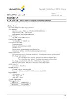
Synergetic Combination of ASIC & Memory ■ 65k colors OLED single chip display driver IC - Serial interface : SPI 4-wire interface - Power save mode - Reduced current driving available - Window mode - Partial display : programmable panel display size - Screen Saver (Vertical scroll, Horizontal panning, Fade in/out ) ■ OLED Column drive - Discharge time control : Discharge time(0clock ~ 30clocks) with internal oscillator clock - Pre-charge peak control : Peak pulse delay time : (Oclock ~ 15clocks) with internal oscillator clock Peak pulse width time : (Oclock ~ 31clocks) with internal oscillator clock - Pre-charge current control : 8-bit, OuA ~ 1020uA by 4uA step control - Driving current control : 8-bit, OuA ~ 188.7uA by 0.74uA step control - Internal / External clock selectable - Frame rate : 95 frames/sec (80.0 ~ 140.0 frames/sec adjustable)
Open the catalog to page 1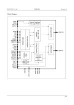
PSEL VSSH VCC_R VCC_C Timing Controller Instruction Registers OSC1 OSC2 VCC_C VCC_R VSSH VDDIO VDD VDDR VSS PD[15:0] ENABLE HSYNC VSYNC DOTCLK VSYNCO RSTB C80 PS CSB A0 RDB/E WRB/RW DB[15:0] Internal Regulator For Logic Power Internal Regulator For ScanDriver BPRE GPRE RPRE
Open the catalog to page 2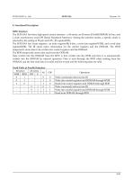
4. Functional Description MPU Interface The SEPS114A has three high-speed system interface : a 68-serise, an 80-serise 8/16/6(RGB/BGR) bit bus, and a clock synchronous serial SPI (Serial Peripheral Interface). Among the interface modes, a specific mode is selected by the setting of PS pin and CPU_IF register(0Dh). The SEPS114A has 3-type registers : an index register(IR) 8-bits, a write data register(WDR), and a read data register(RDR). The IR stores index information for the control registers and the DDRAM. The WDR temporarily stores data to be written into control registers and the DDRAM. The...
Open the catalog to page 4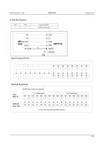
Index/Command Write DDRAM Read/Write
Open the catalog to page 5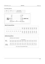
1 Pixel : 65k color with 16-bit MPU interface DDRAM write data
Open the catalog to page 6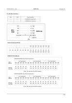
1 Pixel : 65k color with 6-bit MPU interface
Open the catalog to page 7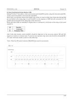
5) Clock Synchronized Serial Interface (SPI) Setting PS to the '0' level allows clock synchronized serial data(SPI) transfer, using the chip select pin(CSB) , A0 pin, serial clock pin(SCL) and serial data input(SDI). When chip is not selected, internal shift register and counter are reset to initial value. Input data through SDI pin are latched at the rising edge of serial clock(SCL) in the sequence of MSB first and converted to 8 -bit parallel data and handled at the rising edge of last serial clock. Serial data input (SDI) are identified to display data or command by A0 bit data at the rising...
Open the catalog to page 8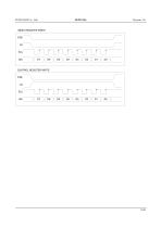
INDEX REGISTER WRITE CSB A0 SCL SDI CONTROL REGISTER WRITE CSB A0 SCL SDI
Open the catalog to page 9
6) RGB Interface When the RGB_IF register(E0h) bit0 is set to “1”, SEPS114A enters into the RGB interface mode and DDRAM write cycle is synchronized by DOTCLK. 1-Image Description VSYNC Pulse Width DDRAM Write Width 8-bit RGB interface The 8-bit RGB interface is selected by setting RIM[1:0] bits to “00”. DDRAM write operation is synchronized with DOTCLK and ENABLE. Display data are transmitted to DDRAM in synchronization with 8-bit RGB data bus(PD[7:0]) and the data enable(ENABLE). DDRAM Write Data format for 8-bit RGB interfa
Open the catalog to page 10
16-bit RGB interface The 16-bit RGB interface is selected by setting RIM[1:0] bits to “01”. DDRAM write operation is synchronized with DOTCLK and ENABLE. Display data are transmitted to DDRAM in synchronization with 16-bit RGB data bus (PD[15:0]) and the data enable (ENABLE). Data format for 16-bit RGB interface Description HSYNC Pulse Width Setup time for Data transfer Hold time for Data transfer DDRAM Write Width
Open the catalog to page 11
6-bit RGB interface The 6-bit RGB interface is selected by setting RIM[1:0] bits to “10”. DDRAM write operation is synchronized with DOTCLK and ENABLE. Display data are transmitted to DDRAM in synchronization with 6-bit RGB data bus(PD[5:0]) and the data enable(ENABLE). DDRAM Write 1st Transmission PD 5 Data format for 6-bit RGB interface Description HSYNC Pulse Width Setup time for Data transfer Hold time for Data transfer DDRAM Write Width
Open the catalog to page 12
6-bit BGR interface The 6-bit BGR interface is selected by setting RIM[1:0] bits to “11”. DDRAM write operation is synchronized with DOTCLK and ENABLE. Display data are transmitted to DDRAM in synchronization with 6-bit RGB data bus(PD[5:0]) and the data enable(ENABLE). VSS DDRAM Write 1st Transmission PD 5 Data format for 6-bit BGR interface Description HSYNC Pulse Width Setup time for Data transfer Hold time for Data transfer DDRAM Write Width
Open the catalog to page 13
The DDRAM stores pixel data for the display. It is composed of 96-row by 96-column x 16-bit addressable array. Address counter provides row and column address to DDRAM for access display pixel data from
Open the catalog to page 14
Window Address Function for DDRAM Write When data is written to the on-chip DDRAM, a window address-range which is specified by the horizontal address register(start : XS[6:0], end : XE[6:0]) or the vertical address register(start : YS[6:0], end : YE[6:0]) can be written to consecutively. Data is written to addresses in the direction specified by the MDIR1, MDIR0(increment/decrement), and VH bit(V or H direction). When the image data is being written, data can be written consecutively without thinking of a data wrap by doing this. The window must be specified within the DDRAM address area described...
Open the catalog to page 15
Reset Status The SEPS114A is initialized as following description when RSTB pin is set to "L". Usually RSTB pin is connected reset pin of MPU, so that the chip can be initialized simultaneously with MPU. The SEPS114A should be initialized when the power is on. INITIAL SETTING CONDITION (default setting) 5. DDRAM write horizontal address : XS = 00h, XE = 5Fh 6. DDRAM write vertical address : YS = 00h, YE = 5Fh 7. Display data RAM write : MDIR1 = 0, MDIR0 = 0, VH = 0 11. Panel display size : FX = 00h, TX = 5Fh, FY = 00h, TY = 5Fh 12. Display data RAM read column/row address : DX = 00h, DY = 00h...
Open the catalog to page 16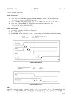
POWER ON/OFF SEQUENCE Power ON sequence (1) Power ON VDD, VDDIO. (2) After VDD, VDDIO become stable and wait for 100ms(t1), set RSTB pin LOW (logic low) for at least 1ms (t2) and then HIGH(logic high). (3) After set RSTB pin HIGH (logic high), wait for at least 50ms (t3). Then Power ON VCC_C (4) After VCC_C become stable, set register 0x02 with value 0x01 for display ON. Data/Scan will be ON after 200ms (tAF). Power OFF sequence (1) Set register 0x02 with value 0x00 for display OFF. (2) Power OFF VCC_C (3) Wait for tOFF. Power OFF VDD, VDDIO (where Minimum tOFF=0ms, Typical tOFF=100ms) On VDD/...
Open the catalog to page 17All NEWHAVEN DISPLAY INTERNATIONAL catalogs and technical brochures
 FT5426G
19 Pages
 FT5336GQQ
13 Pages
 FT5x16
15 Pages
 PT6324
5 Pages
 PT6321
6 Pages
 PT6314
42 Pages
 PT6302
43 Pages
 HT16528
40 Pages
 ILI9341V
249 Pages
 ST7735S
201 Pages
 ST7735P3
197 Pages
 EK79202D
78 Pages
 LT6911C
21 Pages
 SSD1306
59 Pages
 SSD1305
70 Pages
 SEPS525
46 Pages
 SSD1333
36 Pages
 SSD1353
75 Pages
 IST3602
64 Pages
 SSD1333
36 Pages
 SSD1353
75 Pages