IST3602
1 /64Pages
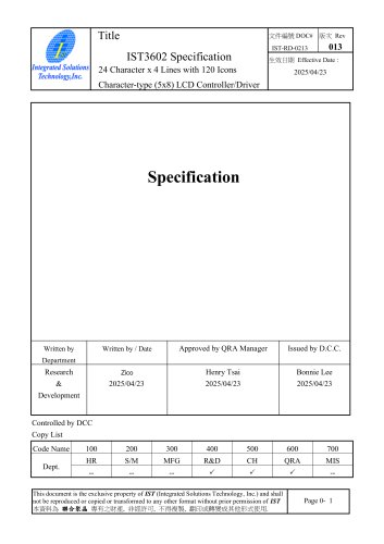
IST3602
1 /64Pages
Catalog excerpts
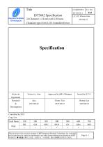
生效日期 Effective Date : 24 Character x 4 Lines with 120 Icons Controlled by DCC Copy List Code Name Dept. This document is the exclusive property of IST (Integrated Solutions Technology, Inc.) and shall not be reproduced or copied or transformed to any other format without prior permission of IST 本資料為 聯合聚晶 專
Open the catalog to page 1
Integrated Solutions Technology,Inc. TitleIST3602 Specification24 Character x 4 Lines with 120 IconsCharacter-type (5x8) LCD Controller/Drivei doc# Effective Date :
Open the catalog to page 2
Integrated Solutions Technology,Inc. TitleIST3602 Specification24 Character x 4 Lines with 120 IconsCharacter-type (5x8) LCD Controller/Drivei doc# This document is the exclusive property of 1ST (Integrated Solutions Technology, Inc.) and shall not be reproduced or copied or transformed to any other format without prior permission of 1ST
Open the catalog to page 3
Integrated Solutions Technology 24 Character x 4 Lines with 120 Icons Character-type (5x8) LCD Controller/Driver INTRODUCTION IST3602 is a character display controller and driver LSI for dot-matrix liquid crystal display. It’s especially designed for VA & EBN LCD Display Module, It can display alphanumeric, Japanese kana and symbols, which are store in the internal Character Generator ROM. It can be configured by a microprocessor with 8-bit parallel interface (6800/8080 series MPU), 3-Line/4-Line serial interface or I2C interface. IST3602 is designed for low voltage supplied applications especially...
Open the catalog to page 4
Integrated Solutions Technology IST3602 Power Supply - Logic Power VDD1 -GROUND = 1.8V ~ 3.6V -Analog Power VDD2 -GROUND = 2.4V ~ 3.6V -Analog Power VDD3 -GROUND = 2.4V ~ 3.6V - 33 common outputs / 120 segment outputs - Display Duty = 1/9,1/17,1/25 1/33 select by command HLINE and NLINE On-chip Display CGROM(Character Generator) - On-chip oscillator circuit for display clock (external clock can also be used) - High performance voltage converter (with - High accuracy reference voltage generator - Electronic contrast control (64 steps) - Embedded V0 Voltage regulator - High performance voltage...
Open the catalog to page 5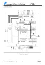
Integrated Solutions Technology BLOCK DIAGRAM DISPLAY DATA CONTROL CIRCUIT 120 SEGMENT DRIVER CIRCUITS 16 COMMON DRIVER CIRCUITS 16 COMMON DRIVER CIRCUITS COMMON OUTPUT CONTROL CIRCUIT V/F CIRCUIT ICCON RAM 24X5=120 Bits V0I DISPLAY TIMING GENERATOR CIRCUIT STATUS REGISTER INSTRUCTION REGISTER INSTRUCTION REGISTER MPU INTERFACE (PARALLEL & SERIAL) Figure 1 Block Diagram
Open the catalog to page 6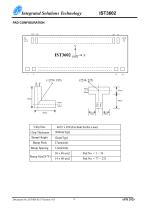
Integrated Solutions Technology IST3602 Chip Size
Open the catalog to page 7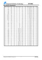
Integrated Solutions Technology IST3602PAD CENTER COORDINATES Pad No.
Open the catalog to page 8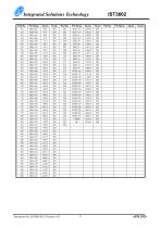
Integrated Solutions Technology IST3602 Pad No.
Open the catalog to page 9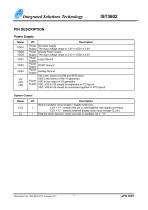
Integrated Solutions Technology IST3602
Open the catalog to page 10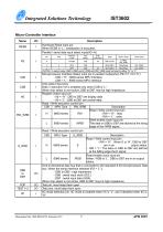
Integrated Solutions Technology IST3602
Open the catalog to page 11
Integrated Solutions Technology IST3602
Open the catalog to page 12
Integrated Solutions Technology IST3602 I/O PIN ITO Resister Limitation PIN Name
Open the catalog to page 13
Integrated Solutions Technology IST3602 There are CSB pins for chip selection. The IST3602 can interface with an MPU only when CSB is “L” . When these pins are set to any other combination, A0, E_RDB, and RW_WRB inputs are disabled and DB0 to DB7 are high impedance. In case of serial interface, the internal shift registers and the counter are reset.
Open the catalog to page 14
Integrated Solutions Technology Serial Interface (IIC=“H” PS = “L”) When IIC = “H” PS = “L”, the IST3602 is configured as Serial interface(4-line or 3-line), the serial data can be input through DB7 (SDA) and serial clock can be input through DB6 (SCL). When the chip is not selected, the shift register & serial data counter will be reset and SDA & SCL will also be disabled internally. 4-Line Serial Interface (IIC=“H” PS = “L” C68=“L”) When the chip is selected (CSB=”L”), the serial data can be shifted in sequentially at the rising edge of SCL and transferred to 8-bit parallel data internally;...
Open the catalog to page 15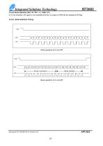
Integrated Solutions Technology 3-Line Serial Interface (IIC=“H” PS = “L” C68=“H”) In 3-Line interface, A0 signal is not available and the 1st output of SDA will be treated as A0 flag. 3-Line Serial Interface Timing Read outdata
Open the catalog to page 16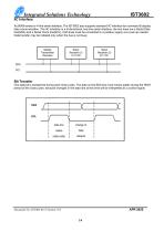
Integrated Solutions Technology IIC Interface As 80/68-sreies or 4-line serial interface, The IST3602 also supports standard IIC interface for command & display data communication. The IIC interface is a bi-directional, two-line serial interface, the two lines are a Serial Data line(SDA) and a Serial Clock line(SCL), both lines must be connected to a positive supply via a pull-up resistor. Data transfer may be initiated only when the bus is not busy. Bit Transfer One data bit is transferred during each clock pulse. The data on the SDA line must remain stable during the HIGH period of the clock...
Open the catalog to page 17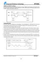
Integrated Solutions Technology START and STOP Conditions Both data and clock lines remain HIGH when the bus is not busy. A HIGH-to-LOW transition of the data line, while the clock is HIGH is defined as the START condition (S). A LOW-to-HIGH transition of the data line while the clock is HIGH is defined as the STOP condition (P). ACKNOWLEDGE Each byte of eight bits is followed by an acknowledge bit. The acknowledge bit is a HIGH signal put on the bus by the transmitter (to release the SDA control and waiting for receiver's ACK), during which time the master generates an extra acknowledge related...
Open the catalog to page 18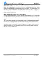
Integrated Solutions Technology IIC Interface Protocol The IIC transmitting is initiated with a START condition (S) from the IIC–bus Master and followed by a slave address. Four 7-bit slave address (0111100, 0111101, 0111110, 0111111) are reserved for the IST3602. The least significant bit of the slave address (ID) is configured by C68 and PS pin to decide is the slave address is 0111100 (C68=0/PS=0) or 0111101 (C68=0/PS=1) or 0111110(C68=1/PS=0) or 0111111(C68=1/PS=1). The 8th bit follows the previous 7-bit address is the data direction bit (R/W) -- '0' indicates Master data transmission (WRITE),...
Open the catalog to page 19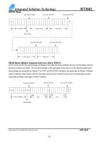
Integrated Solutions Technology WRITE Mode Ack from IST3602 Slave Address Control byte Data byte Write Mode Control byte Data byte READ Mode (Master requests data from Slave, R/W=1) At the moment of the first acknowledge, the Master-transmitter becomes a Master-receiver and the Slave-receiver becomes a Slave transmitter. The first acknowledge is still generated by the slave, but the following data bytes' acknowledge are generated by Master. The STOP and Re-START conditions are generated by Master. If Master wants to stop the data request, after the last data byte has been received, send a Non-Acknowledge...
Open the catalog to page 20All NEWHAVEN DISPLAY INTERNATIONAL catalogs and technical brochures
 FT5426G
19 Pages
 FT5336GQQ
13 Pages
 FT5x16
15 Pages
 PT6324
5 Pages
 PT6321
6 Pages
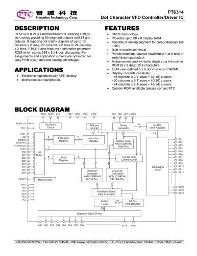 PT6314
42 Pages
 PT6302
43 Pages
 HT16528
40 Pages
 ILI9341V
249 Pages
 ST7735S
201 Pages
 ST7735P3
197 Pages
 EK79202D
78 Pages
 LT6911C
21 Pages
 SSD1306
59 Pages
 SSD1305
70 Pages
 SEPS525
46 Pages
 SEPS114
43 Pages
 SSD1333
36 Pages
 SSD1353
75 Pages
 SSD1333
36 Pages
 SSD1353
75 Pages