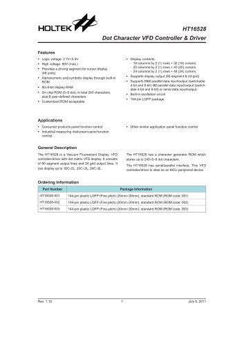
HT16528
1 /40Pages
HT16528
1 /40Pages
Catalog excerpts
• Provides a driving segment for cursor display (48 units) • Alphanumeric and symbolic display through built-in ROM • On chip ROM (5x8 dot), in total 240 characters, plus 8 user-defined characters • Consumer products panel function control • Industrial measuring instrument panel function control The HT16528 is a Vacuum Fluorescent Display, VFD controller/driver with dot matrix VFD display. It consists of 80 segment output lines and 24 grid output lines. It can display up to 16Cx2L, 20Cx2L, 24Cx2L. • Display contents: - 16 columns by 2 (1) rows + 32 (16) cursors - 20 columns by 2 (1) rows + 40 (20) cursors - 24 columns by 2 (1) rows + 48 (24) cursors • Supports display output (80-segment & 24-grid) • Supports M68 parallel data input/output (switchable 4-bit and 8-bit) i80 parallel data input/output (switch-able 4-bit and 8-bit) or serial data input/output • Built-in oscillation circuit • Other similar application panel function control The HT16528 has a character generator ROM which stores up to 240x5x8 dot characters. The HT16528 has serial/parallel interface. This VFD controller/driver is ideal as an MCU peripheral device. Part Number
Open the catalog to page 1
Table 1-3. The Number Of Segment Pins 1
Open the catalog to page 5
Table 1-4. The Number Of Segment Pins 2
Open the catalog to page 6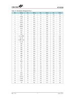
Table 1-5. The Number Of Segment Pins 3
Open the catalog to page 7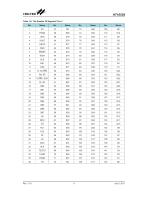
Table 1-6. The Number Of Segment Pins 4
Open the catalog to page 8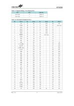
Table 1-7. Segment Setting: 1 Line Display (N=0)
Open the catalog to page 9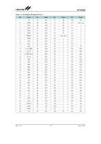
Table 1-9. The Number Of Segment Pins 6
Open the catalog to page 10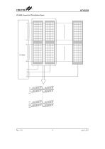
HT16528 HT16528 Connect to VFD as Below Figure
Open the catalog to page 11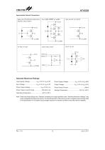
HT16528 Approximate Internal Connections (M P U ) (R S , S T ) (C S ) (D L S ) (D S 0 ) (D S 1 ) (IM ) (R L 1 ) (R L 2 ) (T E S T I)
Open the catalog to page 12
D.C. Characteristics Unless otherwise specified, Vh=50V, Vss=Vlgnd=Vpgnd=0V, Ta=—40oC~85oC Switching Timing
Open the catalog to page 13
Timing Conditions 1 for M68-Type for Parallel Mode, Write Ta=25°C
Open the catalog to page 14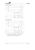
HT16528 Parallel Mode (M68 Input) R S Parallel Mode (M68 Output) R S The input signal rising time and falling time (tf, tr) is specified at 15ns or less. All timing is specified using 20% and 80% of VDD as the reference. PWEH is specified as the overlap between CS being L and E.
Open the catalog to page 15
Timing Conditions 2 for i80-Type, Parallel Mode Ta=25°C
Open the catalog to page 16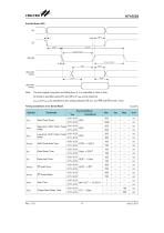
The input signal rising time and falling time (tf, tr) is specified at 15ns or less. All timing is specified using 20% and 80% of VDD as the reference. tCCLW and tCCLR are specified as the overlap between CS as L and WR and RD at the L level. Timing Conditions 3 for Serial Mode Symbol Shift Clock Cycle High-level Shift Clock Pulse 4.5V~5.5V SCK Width 2.7V~4.5V Low-level Shift Clock Pulse 4.5V~5.5V SCK Width 2.7V~4.5V tHSTBK tDS tDK tDKSTB tWSTB tWAIT tODO Shift Clock Hold Time Data Setup Time Data Hold Time Wait Time Output Data Delay Time STD¯ ® SCK¯ Data ® SCK SCK ® Data SCK ® ST
Open the catalog to page 17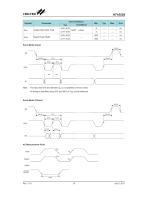
Test Conditions Output Data Hold Time Reset Pulse Width Serial Mode (Input) tW The input rise time and fall time (tR, tF) is specified at 15ns or less. All timing is specified using 20% and 80% of VDD as the reference. Serial Mode (Output)
Open the catalog to page 18
Timing Condition for interface: M68, i80 and Serial Power On Reset Ta=25°C Power Supply Connection Sequence • Connect the PGND and LGND externally to have an equal potential voltage • To avoid faulty connection, turn on the driver power supply (VH) after turning on the logic power supply (VDD). Then turn off the logic power supply (VDD) after turning off the driver power supply (VH). • If the power connection sequence recommended by Holtek is not followed, there's a possibility that the internal logic transistors may be damaged.
Open the catalog to page 19
HT16528 have 4 or 8-bit parallel interface or serial interface. These modes are selected by IM pin. Busy flag data (DB7) is always output as "0". The Address counter (AC) assigns address to both DDRAM and CGRAM. When an instruction address is written into the IR, the address information is sent from the IR to the AC. Selection of either DDRAM or CGRAM is also determined concurrently by the instruction. After writing into (or read from) the DDRAM or CGRAM, the AC is automatically incremented by 1 (or decremented by 1). The cursor position are then output to DB0~DB6 when RS-0 and R, W=1 (Refer...
Open the catalog to page 20
Display Data RAM (DDRAM) The Display data RAM (DDRAM) stores display data represented in 8-bit character codes. Its extended capacity is 80x8 bits or 80 characters. The area in the DDRAM that is not used fordisplay can be used as general data RAM. Refer to DDRAM address table for the relationships between DDRAM address and positions on the VFD. 1-line display (N=0) Display Position (Digit) DDRAM Address (Hexadecimal) The DDRAM address (ADD) is set in the address counter (AC) as hexadecimal. DDRAM Address (Hexadecimal)
Open the catalog to page 21
HT16528 Character Generator ROM (CGROM) ♦ CGROM for generating character patterns of 5x8 dots from 8-bit character codes, generates 240 type of character patterns. ♦ The character codes are shown on the following page. ♦ Character codes 00H to 0FH are allocated to the CGRAM Character Code Table 1 (ROM Code: 001)
Open the catalog to page 23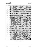
SI Character Code Table 2 (ROM Code: 002)
Open the catalog to page 24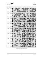
Character Code Table 3 (ROM code: 003)
Open the catalog to page 25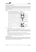
The CGRAM stores the pixel information (1=pixel on, 0=pixel off) for the eight user-define 5x8 characters. Valid CGRAM addresses are 00H to 3FH. CGRAM not used to defined characters can be used as general purpose RAM. Character codes 00H~07H (or08H~0FH) are assigned to the user-defined characters (see section 5.0 character font tables). The table below shows the relationship between the character codes, CGRAM addresses, and CGRAM data for each user-defined character. Relationship between CGRAM address and character code (DDRAM) and 5x7 (with cursor) dot character patterns (CGRAM) CGRAM Data Character...
Open the catalog to page 26
VFD driver circuit consists of 24 grid signal drivers and 80 segment signal drivers. When the character font and number of digits are selected by hardware (DS0, DS1) at power on, the required grid signal drivers automatically output drive waveforms, while the other grid signal driver continue to output non-selection waveforms. Sending serial data is latched when the display data character pattern corresponds to the last address of the display data RAM (DDRAM). Since serial data is latched when the display data character pattern corresponds to the starting address enters the internal shift register,...
Open the catalog to page 27All NEWHAVEN DISPLAY INTERNATIONAL catalogs and technical brochures
 FT5426G
19 Pages
 FT5336GQQ
13 Pages
 FT5x16
15 Pages
 PT6324
5 Pages
 PT6321
6 Pages
 PT6314
42 Pages
 PT6302
43 Pages
 ILI9341V
249 Pages
 ST7735S
201 Pages
 ST7735P3
197 Pages
 EK79202D
78 Pages
 LT6911C
21 Pages
 SSD1306
59 Pages
 SSD1305
70 Pages
 SEPS525
46 Pages
 SEPS114
43 Pages
 SSD1333
36 Pages
 SSD1353
75 Pages
 IST3602
64 Pages
 SSD1333
36 Pages
 SSD1353
75 Pages