EK79202D
1 /78Pages
EK79202D
1 /78Pages
Catalog excerpts
2052CH Source Driver with TCON MIPI/LVDS Interface fitipower integrated technology Inc.
Open the catalog to page 1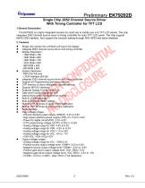
The EK79202 is a highly integrated solution for small size to middle size a-Si TFT-LCD panels. This chip integrates 2052 channel source driver a timing controller for color TFT LCD panel. The chip support MIPI/LVDS interface. And support the function setting through R/W SPI/3-wie serial interface • Single chip solution for a WXGA a-Si type LCD display • Integrate 2052 channel source driver and timing controller • Display Resolution : • System Interfaces: Integrate 2052 channel source driver and timing controller Support for Programming Gamr OTP memory to store initializ Support SPI/I2C interface...
Open the catalog to page 4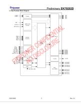
Preliminary EK79202D 3. Chip Function Block Diagram VGMP VGMN MIPI/LVDS Decoder Source Driver POWER converter Timing Controller VCL VGMP VGMN VGL_REG VGH_REG VDD_15V VDD_15V_IF
Open the catalog to page 5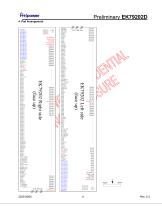
EK79202 Left side (face up) EK79202 Right side (face up)
Open the catalog to page 6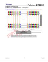
Preliminary EK79202D 5. Application Diagram with Panel 5.1 GIP Application_1366RGBx768 (Normal Dual Gate Driving) Driving method : Cascade=0 Data1 EK79202 IC Bump side down (2052CH) Disable channel -
Open the catalog to page 7
Preliminary EK79202D 5.2 GIP Application_1280RGBx800 (Normal Dual Gate Driving) Driving method : Cascade=0 Data1 EK79202 IC Bump side down (2052CH)
Open the catalog to page 8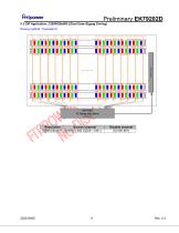
Preliminary EK79202D 5.3 GIP Application_1280RGBx800 ((Dual Gate+Zigzag Driving) Driving method : Cascade=0 Data1 EK79202 IC Bump side down (2052CH)
Open the catalog to page 9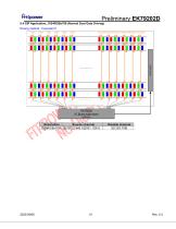
Preliminary EK79202D 5.4 GIP Application_1024RGBx768 (Normal Dual Gate Driving) Driving method : Cascade=0 Data1 EK79202 IC Bump side down (2052CH)
Open the catalog to page 10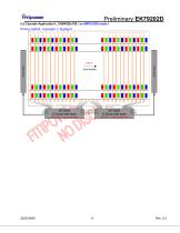
Preliminary EK79202D 5.5 Cascade Application1_1366RGBx768 ( on MIPI/LVDS mode ) Driving method : Cascade=1 / Zigzag=0 Data1 EK79202 IC Bump side down SDLOC=H : chip on left side Scan direction EK79202 IC Bump side down SDLOC=L : chip on right side
Open the catalog to page 11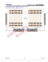
Preliminary EK79202D 5.6 Cascade Application2_1366RGBx768 ( on MIPI/LVDS mode ) Driving method : Cascade=1 / Zigzag=1 / ZTYPE=0 Data1 Scan direction EK79202 IC Bump side down SDLOC=H : chip on left side EK79202 IC Bump side down SDLOC=L : chip on right side
Open the catalog to page 12
Preliminary EK79202D 5.7 Cascade Application3_1366RGBx768 ( on MIPI/LVDS mode ) Driving method : Cascade=1 / Zigzag=1 / ZTYPE=1 Data1 Scan direction EK79202 IC Bump side down SDLOC=H : chip on left side EK79202 IC Bump side down SDLOC=L : chip on right side
Open the catalog to page 13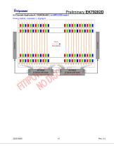
Preliminary EK79202D 5.8 Cascade Application4_1280RGBx800 ( on MIPI/LVDS mode ) Driving method : Cascade=1 / Zigzag=0 Data1 EK79202 IC Bump side down SDLOC=H : chip on left side Scan direction EK79202 IC Bump side down SDLOC=L : chip on right side
Open the catalog to page 14
Preliminary EK79202D 5.9 Cascade Application5_1280RGBx800 ( on MIPI/LVDS mode ) Driving method : Cascade=1 / Zigzag=1 / ZTYPE=0 Data1 DIR=H Scan direction EK79202 IC Bump side down SDLOC=H : chip on left side EK79202 IC Bump side down SDLOC=L : chip on right side
Open the catalog to page 15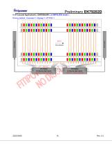
Preliminary EK79202D 5.10 Cascade Application6_1280RGBx800 ( on MIPI/LVDS mode ) Driving method : Cascade=1 / Zigzag=1 / ZTYPE=1 Data1 DIR=H Scan direction EK79202 IC Bump side down SDLOC=H : chip on left side EK79202 IC Bump side down SDLOC=L : chip on right side
Open the catalog to page 16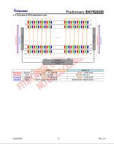
Preliminary EK79202D 5.11 Dual gate & GOA Application note Data1 Backward direction Forward directin Forward directin Backward direction EK79202 IC Bump side down (2052CH) Backward direction Forward direction
Open the catalog to page 17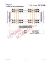
Preliminary EK79202D 5.12 Normal Dual gate & GOA Application note Data1 Backward direction Forward directin Forward directin Backward direction EK79202 IC Bump side down (2052CH) Backward direction Forward direction
Open the catalog to page 18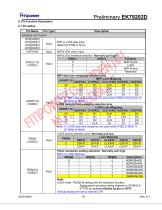
6. Pin Function Description 6.1 Pin define MIPI or LVDS data Input. Select by IFSEL[1:0] pin MIPI/LVDS clock Input. \Note: (1) LVDS data lane sequence are used when IFSEL[1:0]=[0:1] (2) Refer to Note2 LVDS polarity selection pins. Normally pull low. LVDS mode : RES[2:0] setting only for resolution function, Zigzag panel structure setting depend on ZIGZAG & ZTYPE pin selection(Select by pin or OTP) Vertical display line set by internal OTP._
Open the catalog to page 19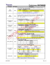
Description The shift direction of device internal shift register is controlled by this as shown below : Normally pull high DIR Function H OUT[0,1,2]‧‧‧OUT[2049,2050,2051] L OUT[2049,2050,2051]‧‧‧OUT[0,1,2] Cascade=H + RES[2:0]=1366x768 only support DIR=H Controls whether the data of D0~D2 are inverted or not, Normally pull low. When “REV”=1 these data will be inverted. EX. “00”→“ 3F”, “07”→“ 38”, “15”→“2A”, and so on. Source OP driving selection: OP_DRV[1:0] (VDDIO) DVCOM_WP (VDDIO) DVCOM_EN (VDDIO) Write protection for internal OTP. Normally High-Z DVCOM_WP Function H Enable write protect...
Open the catalog to page 20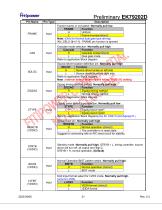
Frame inverse or not select. Normally pull low
Open the catalog to page 21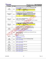
LVBIT (VDDIO) Description 6-bit / 8-bit input select for LVDS mode. Normally pull high. (only for LVDS) LVBIT Function H 8-bit (default) L 6-bit Dithering function enable control. Normally pull low In LVDS 6-bit mode, IC don’t care DITHER and HFRC setting. DITHER_EN (VDDIO) HFRC_EN (VDDIO) H-FRC selection. Normally pull low HFRC = H : H-FRC enable If “DITHER”=”L”,disable dithering function(HFRC and FRC disable) Command interface selection. Normally pull high. CMD_SEL Function H I2C (default) L 3-Wire 3-wire/I2C command can’t receive at the same time. UPDN (VDDIO) Setting flexible GOA scan function....
Open the catalog to page 22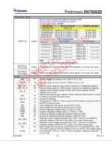
Preliminary EK79202D Panel driver output Source output mapping with different resolution.2051 Source output control by RES[2:0] pin define On Dual gate mode : CAS=0 are used for Panel gate control signals. If not used, let it open. anel gate control signals. If not used, let it open. r supply for analog circuit. VDD=2.3V to 3.6V ;rnal power supply for logic circuits. Connect to a stabilizing capacitor. Internal power supply for LVDS circuits. Connect to a stabilizing capacitor. Interface and I/O power supply for the LVDS power regulator circuits. VDDIO=2.3V to 3.6V. . GND for the internal logic....
Open the catalog to page 23All NEWHAVEN DISPLAY INTERNATIONAL catalogs and technical brochures
 FT5426G
19 Pages
 FT5336GQQ
13 Pages
 FT5x16
15 Pages
 PT6324
5 Pages
 PT6321
6 Pages
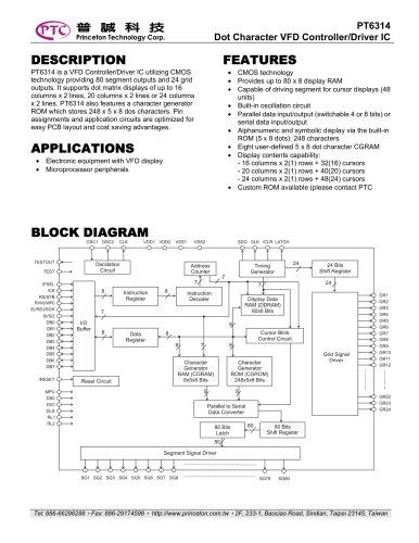 PT6314
42 Pages
 PT6302
43 Pages
 HT16528
40 Pages
 ILI9341V
249 Pages
 ST7735S
201 Pages
 ST7735P3
197 Pages
 LT6911C
21 Pages
 SSD1306
59 Pages
 SSD1305
70 Pages
 SEPS525
46 Pages
 SEPS114
43 Pages
 SSD1333
36 Pages
 SSD1353
75 Pages
 IST3602
64 Pages
 SSD1333
36 Pages
 SSD1353
75 Pages