- Catalogs
- Microchip Technology Inc.
- MCP4801/4811/4821 8/10/12-Bit Voltage Output DAC Converter
MCP4801/4811/4821 8/10/12-Bit Voltage Output DAC Converter
1 /48Pages

MCP4801/4811/4821 8/10/12-Bit Voltage Output DAC Converter
1 /48Pages
Catalog excerpts

„¶ 2010 Microchip Technology Inc. DS22244B-page 1 MCP4801/4811/4821 Features • MCP4801: 8-Bit Voltage Output DAC • MCP4811: 10-Bit Voltage Output DAC • MCP4821: 12-Bit Voltage Output DAC • Rail-to-Rail Output • SPI Interface with 20 MHz Clock Support • Simultaneous Latching of the DAC Output with LDAC Pin • Fast Settling Time of 4.5 ìs • Selectable Unity or 2x Gain Output • 2.048V Internal Voltage Reference • 50ppm/°C VREF Temperature Coefficient • 2.7V to 5.5V Single-Supply Operation • Extended Temperature Range: -40°C to +125°C Applications • Set Point or Offset Trimming • Sensor Calibration • Precision Selectable Voltage Reference • Portable Instrumentation (Battery-Powered) • Calibration of Optical Communication Devices Description The MCP4801/4811/4821 devices are single channel 8-bit, 10-bit and 12-bit buffered voltage output Digital-to-Analog Converters (DACs), respectively. The devices operate from a single 2.7V to 5.5V supply with an SPI compatible Serial Peripheral Interface. The devices have a high precision internal voltage reference (VREF = 2.048V). The user can configure the full-scale range of the device to be 2.048V or 4.096V by setting the Gain Selection Option bit (gain of 1 of 2). The devices can be operated in Active or Shutdown mode by setting a Configuration register bit or using the SHDN pin. In Shutdown mode, most of the internal circuits, including the output amplifier, are turned off for power savings, while the amplifier output (VOUT) stage is configured to present a known high resistance output load (500 kƒÇƒz typicalƒw. The devices include double-buffered registers, allowing a synchronous update of the DAC output using the LDAC pin. These devices also incorporate a Power-on Reset (POR) circuit to ensure reliable powerup. The devices utilize a resistive string architecture, with its inherent advantages of low DNL error, low ratio metric temperature coefficient and fast settling time. These devices are specified over the extended temperature range (+125°C). The devices provide high accuracy and low noise performance for consumer and industrial applications where calibration or compensation of signals (such as temperature, pressure and humidity) are required. The MCP4801/4811/4821 devices are available in the PDIP, SOIC, MSOP and DFN packages. Related Products(1) P/N DAC Resolution No. of Channel Voltage Reference (VREF) MCP4801 8 1 Internal (2.048V) MCP4811 10 1 MCP4821 12 1 MCP4802 8 2 MCP4812 10 2 MCP4822 12 2 MCP4901 8 1 External MCP4911 10 1 MCP4921 12 1 MCP4902 8 2 MCP4912 10 2 MCP4922 12 2 Note 1: The products listed here have similar AC/DC performances. 8/10/12-Bit Voltage Output Digital-to-Analog Converter with Internal VREF and SPI Interface
Open the catalog to page 1
MCP4801/4811/4821 DS22244B-page 2 㦠2010 Microchip Technology Inc. Package Types Block Diagram DFN (2x3)* 1 2 3 4 8 7 6 5 CS SCK SDI VDD VSS VOUT SHDN LDAC MCP4801: 8-bit single DAC MCP4811: 10-bit single DAC MCP4821: 12-bit single DAC MCP48X1 PDIP, SOIC, MSOP 1 2 3 4 8 7 6 5 CS SCK SDI VDD VSS VOUT SHDN LDAC 9 * Includes Exposed Thermal Pad (EP); see Table 3-1. Op Amp VDD VSS CS SDI SCK Interface Logic Input Register DAC Register String DAC Po wer-on Reset VOUT LDAC Output Gain Logic (2.048V) SHDN VREF Output Logic
Open the catalog to page 2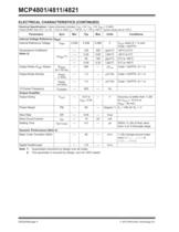
MCP4801/4811/4821 DS22244B-page 4 „¶ 2010 Microchip Technology Inc. Internal Voltage Reference (VREF) Internal Reference Voltage VREF 2.008 2.048 2.088 V VOUT when G = 1x and Code = 0xFFFh Temperature Coefficient (Note 2) ƒ´VREF/°C — 125 325 ppm/°C -40°C to 0°C — 0.25 0.65 LSb/°C -40°C to 0°C — 45 160 ppm/°C 0°C to +85°C — 0.09 0.32 LSb/°C 0°C to +85°C Output Noise (VREF Noise) ENREF (0.1-10 Hz) — 290 — ìVp-p Code = 0xFFFh, G = 1x Output Noise Density eNREF (1 kHz) — 1.2 — ìV/„©Hz Code = 0xFFFh, G = 1x eNREF (10 kHz) — 1.0 — ìV/„©Hz Code = 0xFFFh, G = 1x 1/f Corner Frequency fCORNER — 400 — Hz...
Open the catalog to page 4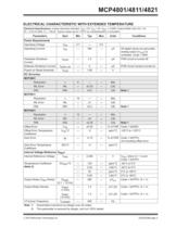
„¶ 2010 Microchip Technology Inc. DS22244B-page 5 MCP4801/4811/4821 ELECTRICAL CHARACTERISTIC WITH EXTENDED TEMPERATURE Electrical Specifications: Unless otherwise indicated, VDD = 5V, VSS = 0V, VREF = 2.048V, Output Buffer Gain (G) = 2x, RL = 5 kƒÇ to GND, CL = 100 pF. Typical values are at +125°C by characterization or simulation. Parameters Sym Min Typ Max Units Conditions Power Requirements Operating Voltage VDD 2.7 — 5.5 Operating Current IDD — 350 — ìA All digital inputs are grounded, analog output (VOUT) is unloaded. Code = 000h Hardware Shutdown Current ISHDN — 1.5 — ìA POR circuit is...
Open the catalog to page 5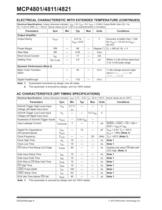
MCP4801/4811/4821 DS22244B-page 6 „¶ 2010 Microchip Technology Inc. Output Amplifier Output Swing VOUT — 0.01 to VDD – 0.04 — V Accuracy is better than 1 LSb for VOUT = 10 mV to (VDD – 40 mV) Phase Margin PM — 66 — Degree (°) CL = 400 pF, RL = „V Slew Rate SR — 0.55 — V/ìs Short Circuit Current ISC — 17 — mA Settling Time tSETTLING — 4.5 — ìs Within ½ LSb of final value from ¼ to ¾ full-scale range Dynamic Performance (Note 2) Major Code Transition Glitch — 45 — nV-s 1 LSb change around major carry (0111...1111 to 1000...0000) Digital Feedthrough — <10 — nV-s AC CHARACTERISTICS (SPI TIMING SPECIFICATIONS)...
Open the catalog to page 6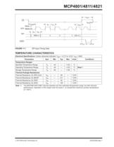
„¶ 2010 Microchip Technology Inc. DS22244B-page 7 MCP4801/4811/4821 FIGURE 1-1: SPI Input Timing Data. TEMPERATURE CHARACTERISTICS Electrical Specifications: Unless otherwise indicated, VDD = +2.7V to +5.5V, VSS = GND. Parameters Sym Min Typ Max Units Conditions Temperature Ranges Specified Temperature Range TA -40 — +125 °C Operating Temperature Range TA -40 — +125 °C Note 1 Storage Temperature Range TA -65 — +150 °C Thermal Package Resistances Thermal Resistance, 8L-DFN (2x3) ƒáJA — 68 — °C/W Thermal Resistance, 8L-MSOP ƒáJA — 211 — °C/W Thermal Resistance, 8L-PDIP ƒáJA — 90 — °C/W Thermal...
Open the catalog to page 7All Microchip Technology Inc. catalogs and technical brochures
 MicroSolutions
8 Pages
 DSA1001/3/4
22 Pages
 Embedded Computing Solutions
4 Pages
 ATmegaET128
469 Pages
 RE46C140
13 Pages
 ATmega4809
74 Pages
 16-bit MCUs and DSCs
20 Pages
 MPLAB® Harmony
12 Pages
 32-bit Microcontroller Family
20 Pages
 32-bit MPU
8 Pages
 UCS100X Family Sell Sheet
2 Pages
 PIC32 Graphics Sell Sheet
2 Pages
 PIC32 Audio Sell Sheet
2 Pages
 PIC1XF150X/155X Sell Sheet
2 Pages
 MRF24WG0MA/MB Sell Sheet
2 Pages
 MCP19111 Sell Sheet
2 Pages
 LAN9730(i) Sell Sheet
2 Pages
 Connectivity Brochure
16 Pages
 bit Embedded Control Solutions
20 Pages


Archived catalogs
 Serial Memory Products
16 Pages
 LIN J2602 Transceiver
32 Pages
 Infrared Encoder/Decoder
36 Pages
 MCP794XX I2C™ RTCC Brochure
2 Pages
 MCP1640/B/C/D
32 Pages
 Motor Control Solutions Brochure
12 Pages
 Power Management MCP1525/41
20 Pages
 PIC32 Overview Brochure
6 Pages
 8-bit PIC® Microcontrollers
16 Pages


- Liebherr signal amplifier
- Liebherr power amplifier
- Wireless module
- Potentiometer
- Liebherr compact converter
- Liebherr serial converter
- Industrial converter
- Manual potentiometer
- Crystal oscillator
- Measuring amplifier
- Liebherr voltage amplifier
- DC amplifier
- Low-noise amplifier
- Power converter
- Precision potentiometer
- Liebherr microcontroller
- Analog amplifier
- Liebherr current amplifier
- Digital converter
- Fast converter