- Catalogs
- Microchip Technology Inc.
- MCP1640/B/C/D
MCP1640/B/C/D
1 /32Pages

MCP1640/B/C/D
1 /32Pages
Catalog excerpts
„¶ 2010 Microchip Technology Inc. DS22234A-page 1 MCP1640/B/C/D Features • Up to 96% Typical Efficiency • 800 mA Typical Peak Input Current Limit: - IOUT > 100 mA @ 1.2V VIN, 3.3V VOUT - IOUT > 350 mA @ 2.4V VIN, 3.3V VOUT - IOUT > 350 mA @ 3.3V VIN, 5.0V VOUT • Low Start-up Voltage: 0.65V, typical 3.3V VOUT @ 1 mA • Low Operating Input Voltage: 0.35V, typical 3.3VOUT @ 1 mA • Adjustable Output Voltage Range: 2.0V to 5.5V • Maximum Input Voltage „T VOUT < 5.5V • Automatic PFM/PWM Operation (MCP1640/C): - PFM Operation Disabled (MCP1640B/D) - PWM Operation: 500 kHz • Low Device Quiescent Current: 19 ìA, typical PFM Mode • Internal Synchronous Rectifier • Internal Compensation • Inrush Current Limiting and Internal Soft-Start • Selectable, Logic Controlled, Shutdown States: - True Load Disconnect Option (MCP1640/B) - Input to Output Bypass Option (MCP1640C/D) • Shutdown Current (All States): < 1 ìA • Low Noise, Anti-Ringing Control • Overtemperature Protection • Available Packages: - SOT23-6 - 2x3 8-Lead DFN Applications • One, Two and Three Cell Alkaline and NiMH/NiCd Portable Products • Single Cell Li-Ion to 5V Converters • Li Coin Cell Powered Devices • Personal Medical Products • Wireless Sensors • Handheld Instruments • GPS Receivers • Bluetooth Headsets • +3.3V to +5.0V Distributed Power Supply General Description The MCP1640/B/C/D is a compact, high-efficiency, fixed frequency, synchronous step-up DC-DC converter. It provides an easy-to-use power supply solution for applications powered by either one-cell, two-cell, or three-cell alkaline, NiCd, NiMH, one-cell Li-Ion or Li-Polymer batteries. Low-voltage technology allows the regulator to start up without high inrush current or output voltage overshoot from a low 0.65V input. High efficiency is accomplished by integrating the low resistance N-Channel Boost switch and synchronous P-Channel switch. All compensation and protection circuitry are integrated to minimize external components. For standby applications, the MCP1640 operates and consumes only 19 ìA while operating at no load and provides a true disconnect from input to output while shut down (EN = GND). Additional device options are available that operate in PWM only mode and connect input to output bypass while shut down. A “true” load disconnect mode provides input to output isolation while disabled by removing the normal boost regulator diode path from input to output. A bypass mode option connects the input to the output using the integrated low resistance P-Channel MOSFET, which provides a low bias keep alive voltage for circuits operating in Deep Sleep mode. Both options consume less than 1 ìA of input current. Output voltage is set by a small external resistor divider. Two package options, SOT23-6 and 2x3 DFN-8, are available. Package Types MCP1640 2x3 DFN* PGND SGND EN VOUTS VOUTP 1 2 3 4 8 7 6 5 SW VFB VIN EP 9 4 1 2 3 6 VIN VFB SW GND EN 5 VOUT MCP1640 6-Lead SOT23 * Includes Exposed Thermal Pad (EP); see Table 3-1. 0.65V Start-up Synchronous Boost Regulator with True Output Disconnect or Input/Output Bypass Option
Open the catalog to page 1
MCP1640/B/C/D DS22234A-page 2 „¶ 2010 Microchip Technology Inc. VIN GND VFB SW VIN 0.9V To 1.7V VOUT 3.3V @ 100 mA COUT 10 ìF CIN 4.7 ìF L1 4.7 ìH VOUT + - 976 KƒÇ 562 KƒÇ ALKALINE VIN PGND VFB SW VIN 3.0V To 4.2V VOUT 5.0V @ 300 mA COUT 10 ìF CIN 4.7 ìF L1 4.7 ìH VOUTS + - 976 KƒÇ 309 KƒÇ VOUTP SGND LI-ION EN EN Efficiency vs. IOUT for 3.3VOUT 40.0 60.0 80.0 100.0 0.1 1.0 10.0 100.0 1000.0 Output Current (mA) Efficiency (%) VIN = 0.8V VIN = 1.2V VIN = 2.5V
Open the catalog to page 2
MCP1640/B/C/D DS22234A-page 4 „¶ 2010 Microchip Technology Inc. TEMPERATURE SPECIFICATIONS NMOS Peak Switch Current Limit IN(MAX) 600 850 — mA Note 5 VOUT Accuracy VOUT% -3 — +3 % Includes Line and Load Regulation; VIN = 1.5V Line Regulation ƒìƒvƒ´VOUT/ VOUT) / ƒ´VIN| -1 0.01 1 %/V VIN = 1.5V to 3V IOUT = 25 mA Load Regulation ƒìƒ´VOUT / VOUT| -1 0.01 1 % IOUT = 25 mA to 100 mA; VIN = 1.5V Maximum Duty Cycle DCMAX 88 90 — % Switching Frequency fSW 425 500 575 kHz EN Input Logic High VIH 90 — — %of VIN IOUT = 1 mA EN Input Logic Low VIL — — 20 %of VIN IOUT = 1 mA EN Input Leakage Current IENLK...
Open the catalog to page 4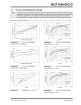
„¶ 2010 Microchip Technology Inc. DS22234A-page 5 MCP1640/B/C/D 2.0 TYPICAL PERFORMANCE CURVES Note: Unless otherwise indicated, VIN = EN = 1.2V, COUT= CIN = 10 ìF, L = 4.7 ìH, VOUT = 3.3V, ILOAD = 15 mA, TA = +25°C. FIGURE 2-1: VOUT IQ vs. Ambient Temperature in PFM Mode. FIGURE 2-2: VOUT IQ vs. Ambient Temperature in PWM Mode. FIGURE 2-3: Maximum IOUT vs. VIN. FIGURE 2-4: 2.0V VOUT PFM / PWM Mode Efficiency vs. IOUT. FIGURE 2-5: 3.3V VOUT PFM / PWM Mode Efficiency vs. IOUT. FIGURE 2-6: 5.0V VOUT PFM / PWM Mode Efficiency vs. IOUT. Note: The graphs and tables provided following this note are...
Open the catalog to page 5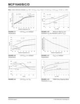
MCP1640/B/C/D DS22234A-page 6 „¶ 2010 Microchip Technology Inc. Note: Unless otherwise indicated, VIN = EN = 1.2V, COUT= CIN = 10 ìF, L = 4.7 ìH, VOUT = 3.3V, ILOAD = 15 mA, TA = +25°C. FIGURE 2-7: 3.3V VOUT vs. Ambient Temperature. FIGURE 2-8: 3.3V VOUT vs. Ambient Temperature. FIGURE 2-9: 3.3V VOUT vs. VIN. FIGURE 2-10: Minimum Start-up and Shutdown VIN into Resistive Load vs. IOUT. FIGURE 2-11: FOSC vs. Ambient Temperature. FIGURE 2-12: PWM Pulse Skipping Mode Threshold vs. IOUT. 3.285 3.29 3.295 3.3 3.305 3.31 3.315 3.32 3.325 3.33 -40 -25 -10 5 20 35 50 65 80 Ambient Temperature (°C) VOUT...
Open the catalog to page 6
„¶ 2010 Microchip Technology Inc. DS22234A-page 7 MCP1640/B/C/D Note: Unless otherwise indicated, VIN = EN = 1.2V, COUT= CIN = 10 ìF, L = 4.7 ìH, VOUT = 3.3V, ILOAD = 15 mA, TA = +25°C. FIGURE 2-13: Input No Load Current vs. VIN. FIGURE 2-14: N-Channel and P-Channel RDSON vs. > of VIN or VOUT. FIGURE 2-15: PFM / PWM Threshold Current vs. VIN. FIGURE 2-16: MCP1640 3.3V VOUT PFM Mode Waveforms. FIGURE 2-17: MCP1640B 3.3V VOUT PWM Mode Waveforms. FIGURE 2-18: MCP1640/B High Load Waveforms. 10 100 1000 10000 0.8 1.1 1.4 1.7 2 2.3 2.6 2.9 3.2 3.5 VIN (V) IIN (ìA) VOUT = 2.0V VOUT = 3.3V VOUT = 5.0V...
Open the catalog to page 7All Microchip Technology Inc. catalogs and technical brochures
 MicroSolutions
8 Pages
 DSA1001/3/4
22 Pages
 Embedded Computing Solutions
4 Pages
 ATmegaET128
469 Pages
 RE46C140
13 Pages
 ATmega4809
74 Pages
 16-bit MCUs and DSCs
20 Pages
 MPLAB® Harmony
12 Pages
 32-bit Microcontroller Family
20 Pages
 32-bit MPU
8 Pages
 UCS100X Family Sell Sheet
2 Pages
 PIC32 Graphics Sell Sheet
2 Pages
 PIC32 Audio Sell Sheet
2 Pages
 PIC1XF150X/155X Sell Sheet
2 Pages
 MRF24WG0MA/MB Sell Sheet
2 Pages
 MCP19111 Sell Sheet
2 Pages
 LAN9730(i) Sell Sheet
2 Pages
 Connectivity Brochure
16 Pages
 bit Embedded Control Solutions
20 Pages


Archived catalogs
 Serial Memory Products
16 Pages
 LIN J2602 Transceiver
32 Pages
 Infrared Encoder/Decoder
36 Pages
 MCP794XX I2C™ RTCC Brochure
2 Pages
 Motor Control Solutions Brochure
12 Pages
 Power Management MCP1525/41
20 Pages
 PIC32 Overview Brochure
6 Pages
 8-bit PIC® Microcontrollers
16 Pages


- Liebherr signal amplifier
- Liebherr power amplifier
- Wireless module
- Potentiometer
- Liebherr compact converter
- Liebherr serial converter
- Industrial converter
- Manual potentiometer
- Crystal oscillator
- Measuring amplifier
- Liebherr voltage amplifier
- DC amplifier
- Low-noise amplifier
- Power converter
- Precision potentiometer
- Liebherr microcontroller
- Analog amplifier
- Liebherr current amplifier
- Digital converter
- Fast converter