- Catalogs
- Microchip Technology Inc.
- LIN J2602 Transceiver
LIN J2602 Transceiver
1 /32Pages

LIN J2602 Transceiver
1 /32Pages
Catalog excerpts

„¶ 2010 Microchip Technology Inc. DS22230C-page 1 MCP2003/4 Features • The MCP2003 and MCP2004 are compliant with LIN Bus Specifications 1.3, 2.0 and 2.1 and are compliant to SAE J2602 • Support Baud Rates up to 20 Kbaudƒnwith LIN-compatible output driver • 43V load dump protected • Very low EMI meets stringent OEM requirements • Very high ESD immunity: - >20kV on VBB (IEC 61000-4-2) - >14kV on LBUS (IEC 61000-4-2) • Very high immunity to RF disturbances meets stringent OEM requirements • Wide supply voltage, 6.0V-27.0V continuous • Extended Temperature Range: -40 to +125°C • Interface to PIC® MCU EUSART and standard USARTs • Local Interconnect Network (LIN) bus pin: - Internal pull-up resistor and diode - Protected against battery shorts - Protected against loss of ground - High current drive • Automatic thermal shutdown • Low-power mode: - Receiver monitoring bus and transmitter off, (ƒ° 5 ìA) Description This device provides a bidirectional, half-duplex communication physical interface to automotive and industrial LIN systems to meet the LIN bus specification Revision 2.1 and SAE J2602. The device is short circuit and overtemperature protected by internal circuitry. The device has been specifically designed to operate in the automotive operating environment and will survive all specified transient conditions while meeting all of the stringent quiescent current requirements. MCP200X family members: • 8-pin PDIP, DFN and SOIC packages: - MCP2003, LIN-compatible driver, with WAKE pins - MCP2004, LIN-compatible driver, with FAULT/TXE pins Package Types MCP2004 PDIP, SOIC FAULT/TXE CS TXD VBB LBUS 1 2 3 4 8 7 6 5 VSS RXD VREN MCP2003 PDIP, SOIC WAKE CS TXD VBB LBUS 1 2 3 4 8 7 6 5 VSS RXD VREN MCP2003 4x4 DFN* WAKE CS TXD VBB LBUS 1 2 3 4 8 7 6 5 VSS RXD VREN EP 9 MCP2004 4x4 DFN* FAULT/TXE CS TXD VBB LBUS 1 2 3 4 8 7 6 5 VSS RXD VREN EP 9 * Includes Exposed Thermal Pad (EP); see Table 1-1. LIN J2602 Transceiver
Open the catalog to page 1
MCP2003/4 DS22230C-page 2 㦠2010 Microchip Technology Inc. MCP2003 Block Diagram MCP2004 Block Diagram Ratiometric Reference OC Thermal Protection VREN WAKE RXD TXD VBB LBUS VSS ~30 kĂ CS Wake-Up Logic and Power Control Short Circuit Protection Ratiometric Reference OC Thermal Protection VREN FAULT/TXE RXD TXD VBB LBUS VSS ~30 kĂ CS Wake-Up Logic and Power Control Short Circuit Protection
Open the catalog to page 2
„¶ 2010 Microchip Technology Inc. DS22230C-page 3 MCP2003/4 1.0 DEVICE OVERVIEW The MCP2003/4 provides a physical interface between a microcontroller and a LIN bus. This device will translate the CMOS/TTL logic levels to LIN logic level, and vice versa. It is intended for automotive and industrial applications with serial bus speeds up to 20 Kbaud. LIN specification 2.1 requires that the transceiver of all nodes in the system is connected via the LIN pin, referenced to ground and with a maximum external termination resistance of 510ƒÇ from LIN bus to battery supply. The 510ƒÇƒn corresponds to...
Open the catalog to page 3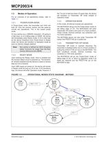
MCP2003/4 DS22230C-page 4 㦠2010 Microchip Technology Inc. 1.3 Modes of Operation For an overview of all operational modes, refer to Table 1-1. 1.3.1 POWER-DOWN MODE In Power-Down mode, the transmitter and VREN are both off. Only the receiver section and the wake-up circuits are operational. This is the lowest power mode. On bus activity (e.g. a BREAK character), CS going to a high level, or on a falling edge on WAKE, the device will immediately enter Ready mode. If CS is held high as the device transitions from Power-Down to Ready mode, the device will transition to Operation mode as soon as...
Open the catalog to page 4
㦠2010 Microchip Technology Inc. DS22230C-page 5 MCP2003/4 FIGURE 1-3: OPERATIONAL MODES STATE DIAGRAM РMCP2004 TABLE 1-1: OVERVIEW OF OPERATIONAL MODES Note: While the MCP2003/4 is in thermal shutdown, TXD should not be actively driven high or it may power internal logic through the ESD diodes and may damage the device. State Transmitter Receiver Vren Operation Comments POR OFF OFF OFF Read CS, if low, then Ready; if high, Operational mode Ready OFF ON ON If CS high level, then Operation mode Bus Off state Operation ON ON ON If CS low level, then Power Down; If FAULT/TXE low level, then Transmitter...
Open the catalog to page 5
MCP2003/4 DS22230C-page 6 „¶ 2010 Microchip Technology Inc. 1.4 Typical Applications EXAMPLE 1-1: TYPICAL MCP2003 APPLICATION EXAMPLE 1-2: TYPICAL MCP2004 APPLICATION LIN Bus 27V VBB LBUS VREN TXD RXD VSS VDD TXD RXD +12 1.0 ìF I/O CS WAKE 50ƒÇ 43V 1 KƒÇ +12 Master Node Only +12 220 KƒÇ Wake-up VOLTAGE REG 100 nF (See Note) Note: For applications with current requirements of less than 20 mA, the connection to +12V can be deleted, and voltage to the regulator supplied directly from the VREN pin. LIN Bus 27V VBB LBUS VREN TXD RXD VSS VDD TXD RXD +12 1.0 ìF I/O CS I/O FAULT/TXE 50ƒÇ 43V 1 KƒÇ +12...
Open the catalog to page 6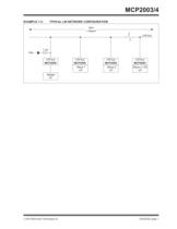
„¶ 2010 Microchip Technology Inc. DS22230C-page 7 MCP2003/4 EXAMPLE 1-3: TYPICAL LIN NETWORK CONFIGURATION Master ìC 1 kƒÇ VBB Slave 1 ìC Slave 2 ìC Slave n <23 ìC 40m + Return LIN bus LIN bus MCP200X LIN bus MCP200X LIN bus MCP200X LIN bus MCP200X
Open the catalog to page 7
MCP2003/4 DS22230C-page 8 㦠2010 Microchip Technology Inc. 1.5 Pin Descriptions TABLE 1-1: PINOUT DESCRIPTIONS 1.5.1 RECEIVE DATA OUTPUT (RXD) The Receive Data Output pin is a open drain (OD) output and follows the state of the LIN pin. 1.5.2 CS (CHIP SELECT) Chip Select Input pin. An internal pull-down resistor will keep the CS pin low. This is done to ensure that no disruptive data will be present on the bus while the microcontroller is executing a Power-on Reset and an I/O initialization sequence. The pin must detect a high level to activate the transmitter. If CS = 0 when the VBB supply...
Open the catalog to page 8
„¶ 2010 Microchip Technology Inc. DS22230C-page 9 MCP2003/4 TABLE 1-2: FAULT/TXE TRUTH TABLE 1.5.5 TRANSMIT DATA INPUT (TXD) The Transmit Data Input pin has an internal pull-up. The LIN pin is low (dominant) when TXD is low, and high (recessive) when TXD is high. For extra bus security, TXD is internally forced to ‘1’ whenever the transmitter is disabled regardless of external TXD voltage. 1.5.5.1 TXD Dominant Timeout If TXD is driven low longer than approximately 10ms, the LBUS pin is switched to recessive mode and the part enters TOFF Mode. This is to prevent the LIN node from permanently driving...
Open the catalog to page 9All Microchip Technology Inc. catalogs and technical brochures
 MicroSolutions
8 Pages
 DSA1001/3/4
22 Pages
 Embedded Computing Solutions
4 Pages
 ATmegaET128
469 Pages
 RE46C140
13 Pages
 ATmega4809
74 Pages
 16-bit MCUs and DSCs
20 Pages
 MPLAB® Harmony
12 Pages
 32-bit Microcontroller Family
20 Pages
 32-bit MPU
8 Pages
 UCS100X Family Sell Sheet
2 Pages
 PIC32 Graphics Sell Sheet
2 Pages
 PIC32 Audio Sell Sheet
2 Pages
 PIC1XF150X/155X Sell Sheet
2 Pages
 MRF24WG0MA/MB Sell Sheet
2 Pages
 MCP19111 Sell Sheet
2 Pages
 LAN9730(i) Sell Sheet
2 Pages
 Connectivity Brochure
16 Pages
 bit Embedded Control Solutions
20 Pages


Archived catalogs
 Serial Memory Products
16 Pages
 Infrared Encoder/Decoder
36 Pages
 MCP794XX I2C™ RTCC Brochure
2 Pages
 MCP1640/B/C/D
32 Pages
 Motor Control Solutions Brochure
12 Pages
 Power Management MCP1525/41
20 Pages
 PIC32 Overview Brochure
6 Pages
 8-bit PIC® Microcontrollers
16 Pages


- Liebherr signal amplifier
- Liebherr power amplifier
- Wireless module
- Potentiometer
- Liebherr compact converter
- Liebherr serial converter
- Industrial converter
- Manual potentiometer
- Crystal oscillator
- Measuring amplifier
- Liebherr voltage amplifier
- DC amplifier
- Low-noise amplifier
- Power converter
- Precision potentiometer
- Analog amplifier
- Liebherr current amplifier
- Digital converter
- Fast converter