- Catalogs
- Microchip Technology Inc.
- DSA1001/3/4
DSA1001/3/4
1 /22Pages

DSA1001/3/4
1 /22Pages
Catalog excerpts
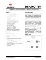
Microchip DSA1001/3/4 1.8V-3.3V Low-Power Precision CMOS Oscillators for Automotive Features • Automotive AEC-Q100 Qualified • Frequency Range: 1 MHz to 150 MHz • Exceptional Stability over Temperature - ±20 ppm, ±25 ppm, ±50 ppm • Operating Voltage - 1.7 to 3.6V • Operating Temperature Range - Automotive Grade 2: -40°C to 105°C - Automotive Grade 3: -40°C to 85°C • Low Operating and Standby Current - 6 mA Operating (1 MHz) - 15 |jA Standby (Max.) • Ultra Miniature Footprint - 2.5 mm x 2.0 mm x 0.85 mm - 3.2 mm x 2.5 mm x 0.85 mm - 5.0 mm x 3.2 mm x 0.85 mm • MIL-STD 883 Shock and Vibration Resistant General Description The DSA1001/3/4 is a silicon MEMS based CMOS family of oscillators that offers excellent jitter and stability performance over a wide range of supply voltages and temperatures. The device operates from 1 MHz to 150 MHz with supply voltages between 1.8 to 3.3 volts and temperature ranges up to -40°C to 105°C. The DSA1001/3/4 incorporate an all silicon resonator that is extremely robust and nearly immune to stress related fractures, common to crystal based oscillators. Without sacrificing the performance and stability required of today's systems, a crystal-less design allows for a higher level of reliability, making the DSA1001/3/4 ideal for rugged, industrial, and portable applications where stress, shock, and vibration can damage quartz crystal based systems. Available in industry standard packages, the DSA1001/3/4 can be “dropped-in” to the same PCB footprint as standard crystal oscillators. • Pb Free, RoHS, Reach SVHC Compliant Applications • Automotive Infotainment • Automotive ADAS • Automotive Camera Module Benefits • Replace High Temperature Crystals and Quartz Oscillators • Pin for Pin “Drop-In” Replacement for Industry Standard Oscillators • Semiconductor Level Reliability, Significantly Higher than Quartz • Longer Battery Life/Reduced Power Consumption • Compact Plastic Package • Cost Effective The DSA1003 and DSA1004 have the same functionality and performance as the DSA1001, but feature higher output drives of 25 pF and 40 pF, respectively. Package Types
Open the catalog to page 1
t Notice: Stresses above those listed under “Absolute Maximum Ratings” may cause permanent damage to the device. This is a stress rating only and functional operation of the device at those or any other conditions above those indicated in the operational sections of this specification is not intended. Exposure to maximum rating conditions for extended periods may affect device reliability. TABLE 1-1: ELECTRICAL CHARACTERISTICS Electrical Characteristics: Vdd = 1.8 to 3.3V; TA = +85°C unless otherwise specified. Note 1: tSu is time to stable output frequency after Vdd is applied. tSu and tEN (after...
Open the catalog to page 3
TABLE 1-1: ELECTRICAL CHARACTERISTICS (CONTINUED) Electrical Characteristics: Vdd = 1.8 to 3.3V; TA = +85°C unless otherwise specified. Note 1: tSU is time to stable output frequency after Vdd is applied. tSU and tEN (after EN is asserted) are identical values. 2: Measured over 50k clock cycles.
Open the catalog to page 4
TABLE 1-1: ELECTRICAL CHARACTERISTICS (CONTINUED)
Open the catalog to page 5
Note 1: The maximum allowable power dissipation is a function of ambient temperature, the maximum allowable junction temperature and the thermal resistance from junction to air (i.e., TA, Tj, 9jA). Exceeding the maximum allowable power dissipation will cause the device operating junction temperature to exceed the maximum +150°C rating. Sustained junction temperatures above +150°C can impact the device reliability.
Open the catalog to page 6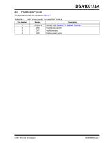
2.0 PIN DESCRIPTIONS The descriptions of the pins are listed in Table 2-1. TABLE 2-1: CDFN PACKAGE PIN FUNCTION TABLE
Open the catalog to page 7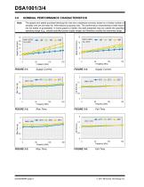
NOMINAL PERFORMANCE CHARACTERISTICS The graphs and tables provided following this note are a statistical summary based on a limited number of samples and are provided for informational purposes only. The performance characteristics listed herein are not tested or guaranteed. In some graphs or tables, the data presented may be outside the specified operating range (e.g., outside specified power supply range) and therefore outside the warranted range. Supply Current. Supply Current. Rise Time. Fall Time. Rise Time. Fall Time.
Open the catalog to page 8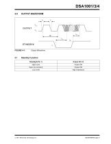
Output Waveform. Standby Function Standby# (Pin 1) High Level High Impedance
Open the catalog to page 9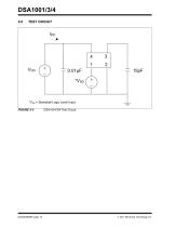
TEST CIRCUIT *VSD = Standby# Logic Level Input FIGURE 5-1:
Open the catalog to page 10
FIGURE 6-1: Recommended Board Layout for DSA1001/3/4.
Open the catalog to page 11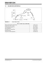
SOLDER REFLOW PROFILE Cool Time Solder Reflow Profile. MSL 1 @ 260°C refer to JSTD-020C Ramp-Up Rate (200°C to Peak Temp) Time maintained above 217°C Peak Temperature Time within 5°C of Actual Peak Ramp-Down Rate Time 25°C to Peak Temperature
Open the catalog to page 12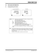
Product code, customer-specific information, or frequency in MHz without printed decimal point Year code (last digit of calendar year) Year code (last 2 digits of calendar year) Week code (week of January 1 is week '01') Alphanumeric traceability code Pb-free JEDEC® designator for Matte Tin (Sn) This package is Pb-free. The Pb-free JEDEC designator (;e3) can be found on the outer packaging for this package. • , ▲, ▼ Pin one index is identified by a dot, delta up, or delta down (triangle mark). Note: In the event the full Microchip part number cannot be marked on one line, it will be carried over...
Open the catalog to page 13
DSA1001/3/4 4-Lead CDFN 5.0 mm x 3.2 mm Package Outline & Recommended Land Pattern
Open the catalog to page 14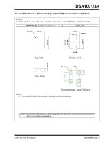
DSA1001/3/4 4-Lead CDFN 3.2 mm x 2.5 mm Package Outline & Recommended Land Pattern
Open the catalog to page 15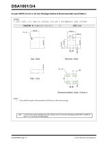
DSA1001/3/4 4-Lead CDFN 2.5 mm x 2.0 mm Package Outline & Recommended Land Pattern
Open the catalog to page 16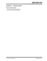
Revision A (March 2018) • Initial release of data sheet DSA1001/3/4 to Microchip format data sheet DS20005889A.
Open the catalog to page 17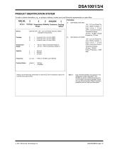
DSA1001/3/4 To order or obtain information, e.g., on pricing or delivery, contact your local Microchip representative or sales office. X XX -XXX.XXXX XPackage Temperature Stability Frequency Packing Range Option Examples: a) DSA1003BL3-030.0000: Device: DSA1001/3/4: 1.8V - 3.3V Low-Power Precision CMOS -40oC to +850C (Automotive Grade 3) -40oC to +1050C (Automotive Grade 2) 1.8V - 3.3V Low-Power Precision CMOS Oscillator, 4-Lead 5.0 mm x 3.2 mm CDFN, Automotive Grade 2 Temperature Range, ±20 ppm, 30 MHz Output Frequency, 72/Tube 1.8V - 3.3V Low-Power Precision CMOS Oscillator, 4-Lead 2.5 mm x...
Open the catalog to page 19All Microchip Technology Inc. catalogs and technical brochures
 MicroSolutions
8 Pages
 Embedded Computing Solutions
4 Pages
 ATmegaET128
469 Pages
 RE46C140
13 Pages
 ATmega4809
74 Pages
 16-bit MCUs and DSCs
20 Pages
 MPLAB® Harmony
12 Pages
 32-bit Microcontroller Family
20 Pages
 32-bit MPU
8 Pages
 UCS100X Family Sell Sheet
2 Pages
 PIC32 Graphics Sell Sheet
2 Pages
 PIC32 Audio Sell Sheet
2 Pages
 PIC1XF150X/155X Sell Sheet
2 Pages
 MRF24WG0MA/MB Sell Sheet
2 Pages
 MCP19111 Sell Sheet
2 Pages
 LAN9730(i) Sell Sheet
2 Pages
 Connectivity Brochure
16 Pages
 bit Embedded Control Solutions
20 Pages


Archived catalogs
 Serial Memory Products
16 Pages
 LIN J2602 Transceiver
32 Pages
 Infrared Encoder/Decoder
36 Pages
 MCP794XX I2C™ RTCC Brochure
2 Pages
 MCP1640/B/C/D
32 Pages
 Motor Control Solutions Brochure
12 Pages
 Power Management MCP1525/41
20 Pages
 PIC32 Overview Brochure
6 Pages
 8-bit PIC® Microcontrollers
16 Pages


- Liebherr signal amplifier
- Liebherr power amplifier
- Wireless module
- Potentiometer
- Liebherr compact converter
- Liebherr serial converter
- Industrial converter
- Manual potentiometer
- Measuring amplifier
- Liebherr voltage amplifier
- DC amplifier
- Low-noise amplifier
- Power converter
- Precision potentiometer
- Liebherr microcontroller
- Analog amplifier
- Liebherr current amplifier
- Digital converter
- Fast converter