- Catalogs
- Microchip Technology Inc.
- ATmega4809
ATmega4809
1 /74Pages

ATmega4809
1 /74Pages
Catalog excerpts
Introduction The ATmega4809 microcontrollers of the megaAVR® 0-series are using the AVR® processor with hardware multiplier, running at up to 20 MHz, with a wide range of Flash sizes up to 48 KB, up to 6 KB of SRAM, and 256 bytes of EEPROM in 28-, 32-, 40-, or 48-pin package. The series uses the latest technologies from Microchip with a flexible and low-power architecture including Event System and SleepWalking, accurate analog features and advanced peripherals. The devices described here offer a Flash size of 48 KB in a 40-pin package. Important: The 40-pin version of the ATmega4809 is using the die of the 48-pin ATmega4809 but offers fewer connected pads. For this reason, the pins PB[5:0] and PC[7:6] must be disabled (INPUT_DISABLE) or enable pull-ups (PULLUPEN). Features • AVR® CPU: - Single-cycle I/O access - Two-level interrupt controller - Two-cycle hardware multiplier • Memories: - Up to 48 KB In-system self-programmable Flash memory - 256B EEPROM - Up to 6 KB SRAM - Write/Erase endurance: • Flash 10,000 cycles • EEPROM 100,000 cycles - Data retention: 40 Years at 55°C • System: - Power-on Reset (POR) circuit - Brown-out Detector (BOD) - Clock options: • 16/20 MHz low-power internal oscillator • 32.768 kHz Ultra Low-Power (ULP) internal oscillator • 32.768 kHz external crystal oscillator • External clock input - Single pin Unified Program Debug Interface (UPDI) - Three Sleep modes: • Idle with all peripherals running for immediate wake-up • Standby - Configurable operation of selected peripherals Preliminary Datasheet
Open the catalog to page 1
– SleepWalking peripherals • Power-Down with limited wake-up functionality Peripherals: – One 16-bit Timer/Counter type A (TCA) with a dedicated period register and three compare channels – Four 16-bit Timer/Counter type B with input capture (TCB) – One 16-bit Real-Time Counter (RTC) running from an external crystal or an internal RC oscillator – Four USART with fractional baud rate generator, auto-baud, and start-of-frame detection – Master/slave Serial Peripheral Interface (SPI) – Dual mode Master/Slave TWI with dual address match • Standard mode (Sm, 100 kHz) • Fast mode (Fm, 400 kHz) • Fast...
Open the catalog to page 2
© 2019 Microchip Technology Inc. Preliminary Datasheet DS40002104B-page 3
Open the catalog to page 3
Preliminary Datasheet
Open the catalog to page 4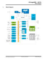
Block Diagram AINPn AINNn OUT AINn VREFA LUTn-INn LUTn-OUT EVSYS CCL TCAn TCBn SDA (master) SCL (master) SDA (slave) SCL (slave) System Management RSTCTRL Detectors/ References RESET RST CLKCTRL SLPCTRL Clock Generation CLKOUT Preliminary Datasheet
Open the catalog to page 5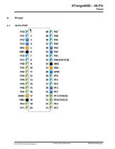
© 2019 Microchip Technology Inc. Preliminary Datasheet DS40002104B-page 6
Open the catalog to page 6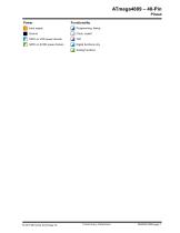
J Ground | | GPIO on VDD power domain | | GPIO on AVDD power domain Functionality a Programming, debug | | Clock, crystal | | Digital functions only © 2019 Microchip Technology Inc. Preliminary Datasheet DS40002104B-page 7
Open the catalog to page 7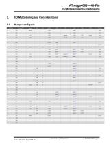
© 2019 Microchip Technology Inc. Preliminary Datasheet DS40002104B-page 8
Open the catalog to page 8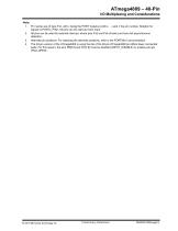
ATmega4809 – 40-Pin I/O Multiplexing and Considerations Note: 1. Pin names are of type Pxn, with x being the PORT instance (A,B,C, ...) and n the pin number. Notation for signals is PORTx_PINn. All pins can be used as event input. 2. All pins can be used for external interrupt, where pins Px2 and Px6 of each port have full asynchronous detection. 3. Alternate pin positions. For selecting the alternate positions, refer to the PORTMUX documentation. 4. The 40-pin version of the ATmega4809 is using the die of the 48-pin ATmega4809 but offers fewer connected pads. For this reason, the pins PB[5:0]...
Open the catalog to page 9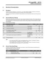
Electrical Characteristics 4.1 Disclaimer All typical values are measured at T = 25°C and VDD = 3V unless otherwise specified. All minimum and maximum values are valid across operating temperature and voltage unless otherwise specified. Typical values given should be considered for design guidance only, and actual part variation around these values is expected. 4.2 Absolute Maximum Ratings Stresses beyond those listed in this section may cause permanent damage to the device. This is a stress rating only and functional operation of the device at these or other conditions beyond those indicated...
Open the catalog to page 10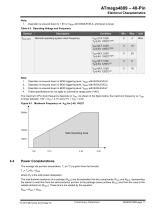
1. Operation is ensured down to 1.8V or VBOD with BODLEVEL0, whichever is lower. Table 4-3. Operating Voltage and Frequency Note: 1. Operation is ensured down to BOD triggering level, VBOD with BODLEVEL0. 2. Operation is ensured down to BOD triggering level, VBOD with BODLEVEL2. 3. Operation is ensured down to BOD triggering level, VBOD with BODLEVEL7. 4. These specifications do not apply to automotive range parts (-VAO). The maximum CPU clock frequency depends on VDD. As shown in the figure below, the maximum frequency vs. VDD is linear between 1.8V < VDD < 2.7V and 2.7V < VDD < 4.5V. Figure...
Open the catalog to page 11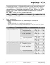
R0JC is device related and cannot be influenced by the user. However, R0CA is user-dependent and can be minimized by thermal management techniques such as heat sinks, ambient air cooling, and thermal convection. Thus, good thermal management on the part of the user can significantly reduce R0CA so that R0JA approximately equals R0JC. The power dissipation curve is negatively sloped as ambient temperature increase. The maximum power dissipation is, therefore, at minimum ambient temperature while the highest junction temperature occurs at the maximum ambient temperature. Table 4-4. Power Dissipation...
Open the catalog to page 12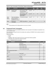
Table 4-6. Power Consumption in Power-Down, Standby and Reset Mode © 2019 Microchip Technology Inc. Preliminary Datasheet DS40002104B-page 13
Open the catalog to page 13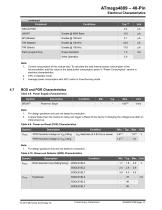
© 2019 Microchip Technology Inc. Preliminary Datasheet DS40002104B-page 14
Open the catalog to page 14
© 2019 Microchip Technology Inc. Preliminary Datasheet DS40002104B-page 15
Open the catalog to page 15
© 2019 Microchip Technology Inc. Preliminary Datasheet DS40002104B-page 16
Open the catalog to page 16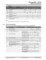
© 2019 Microchip Technology Inc. Preliminary Datasheet DS40002104B-page 17
Open the catalog to page 17
© 2019 Microchip Technology Inc. Preliminary Datasheet DS40002104B-page 18
Open the catalog to page 18All Microchip Technology Inc. catalogs and technical brochures
 MicroSolutions
8 Pages
 DSA1001/3/4
22 Pages
 Embedded Computing Solutions
4 Pages
 ATmegaET128
469 Pages
 RE46C140
13 Pages
 16-bit MCUs and DSCs
20 Pages
 MPLAB® Harmony
12 Pages
 32-bit Microcontroller Family
20 Pages
 32-bit MPU
8 Pages
 UCS100X Family Sell Sheet
2 Pages
 PIC32 Graphics Sell Sheet
2 Pages
 PIC32 Audio Sell Sheet
2 Pages
 PIC1XF150X/155X Sell Sheet
2 Pages
 MRF24WG0MA/MB Sell Sheet
2 Pages
 MCP19111 Sell Sheet
2 Pages
 LAN9730(i) Sell Sheet
2 Pages
 Connectivity Brochure
16 Pages
 bit Embedded Control Solutions
20 Pages


Archived catalogs
 Serial Memory Products
16 Pages
 LIN J2602 Transceiver
32 Pages
 Infrared Encoder/Decoder
36 Pages
 MCP794XX I2C™ RTCC Brochure
2 Pages
 MCP1640/B/C/D
32 Pages
 Motor Control Solutions Brochure
12 Pages
 Power Management MCP1525/41
20 Pages
 PIC32 Overview Brochure
6 Pages
 8-bit PIC® Microcontrollers
16 Pages


- Liebherr signal amplifier
- Liebherr power amplifier
- Wireless module
- Potentiometer
- Liebherr compact converter
- Liebherr serial converter
- Industrial converter
- Manual potentiometer
- Measuring amplifier
- Liebherr voltage amplifier
- DC amplifier
- Low-noise amplifier
- Power converter
- Precision potentiometer
- Analog amplifier
- Liebherr current amplifier
- Digital converter
- Fast converter