- Catalogs
- Microchip Technology Inc.
- 30 µA, High Precision Op Amps (MCP6051/2/4)
30 µA, High Precision Op Amps (MCP6051/2/4)
1 /40Pages

30 µA, High Precision Op Amps (MCP6051/2/4)
1 /40Pages
Catalog excerpts

© 2010 Microchip Technology Inc. DS22182B-page 1 MCP6051/2/4 Features • Low Offset Voltage: ±150 ìV (maximum) • Low Quiescent Current: 30 ìA (typical) • Rail-to-Rail Input and Output • Wide Supply Voltage Range: 1.8V to 6.0V • Gain Bandwidth Product: 385 kHz (typical) • Unity Gain Stable • Extended Temperature Range: -40°C to +125°C • No Phase Reversal Applications • Automotive • Portable Instrumentation • Sensor Conditioning • Battery Powered Systems • Medical Instrumentation • Test Equipment • Analog Filters Design Aids • SPICE Macro Models • FilterLab® Software • Microchip Advanced Part Selector (MAPS) • Analog Demonstration and Evaluation Boards • Application Notes Typical Application Description The Microchip Technology Inc. MCP6051/2/4 family of operational amplifiers (op amps) has low input offset voltage (±150 ìV, maximum) and rail-to-rail input and output operation. This family is unity gain stable and has a gain bandwidth product of 385 kHz (typical). These devices operate with a single supply voltage as low as 1.8V, while drawing low quiescent current per amplifier (30 ìA, typical). These features make the family of op amps well suited for single-supply, high precision, battery-powered applications. The MCP6051/2/4 family is offered in single (MCP6051), dual (MCP6052), and quad (MCP6054) configurations. The MCP6051/2/4 is designed with Microchip’s advanced CMOS process. All devices are available in the extended temperature range, with a power supply range of 1.8V to 6.0V. Package Types RL VOUT Gyrator ZIN R C ZIN = RL + jùL L=RLRC MCP6051 * Includes Exposed Thermal Pad (EP); see Table 3-1. 1 2 3 4 8 7 6 5 EP 9 VDD VOUT NC NC VIN+ VIN– VSS NC 1 2 3 4 8 7 6 5 EP 9 VOUTB VINB– VINB+ VDD VINA+ VINA– VSS VOUTA VINA+ VINA– VDD 1 2 3 4 14 13 12 11 VOUTA VOUTD VIND– VIND+ VSS VINB+ 5 10 VINC+ VINB– 6 9 VOUTB 7 8 VOUTC VINC– VINA+ VINA– VSS 1 2 3 4 8 7 6 5 VOUTA VDD VOUTB VINB– VINB+ VIN+ VIN– VSS 1 2 3 4 8 7 6 5 NC NC VDD VOUT NC MCP6051 SOIC MCP6052 SOIC MCP6051 2x3 TDFN * MCP6054 SOIC, TSSOP MCP6052 2x3 TDFN * VIN+ VIN– VSS 1 2 3 5 4 VOUT VDD MCP6051 SOT-23-5 30 ìA, High Precision Op Amps
Open the catalog to page 1
MCP6051/2/4 DS22182B-page 2 © 2010 Microchip Technology Inc. NOTES:
Open the catalog to page 2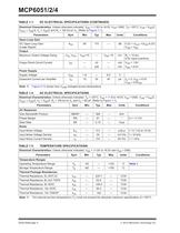
MCP6051/2/4 DS22182B-page 4 © 2010 Microchip Technology Inc. TABLE 1-2: AC ELECTRICAL SPECIFICATIONS TABLE 1-3: TEMPERATURE SPECIFICATIONS Open-Loop Gain DC Open-Loop Gain (Large Signal) AOL 95 115 — dB 0.2V < VOUT <(VDD-0.2V) VCM = VSS Output Maximum Output Voltage Swing VOL, VOH VSS+15 — VDD–15 mV RL = 10 kÙ, 0.5V input overdrive Output Short-Circuit Current ISC — ±5 — mA VDD = 1.8V — ±26 — mA VDD = 6.0V Power Supply Supply Voltage VDD 1.8 — 6.0 V Quiescent Current per Amplifier IQ 15 30 45 ìA IO = 0, VDD = 6.0V VCM = 0.9VDD Electrical Characteristics: Unless otherwise indicated, TA = +25°C,...
Open the catalog to page 4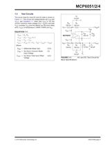
© 2010 Microchip Technology Inc. DS22182B-page 5 MCP6051/2/4 1.3 Test Circuits The circuit used for most DC and AC tests is shown in Figure 1-1. This circuit can independently set VCM and VOUT; see Equation 1-1. Note that VCM is not the circuit’s common mode voltage ((VP + VM)/2), and that VOST includes VOS plus the effects (on the input offset error, VOST) of temperature, CMRR, PSRR and AOL. EQUATION 1-1: FIGURE 1-1: AC and DC Test Circuit for Most Specifications. GDM = RF RG VCM = (VP + VDD 2) 2 VOUT = (VDD 2)+(VP – VM)+VOST(1+GDM) Where: GDM = Differential Mode Gain (V/V) VCM = Op Amp’s Common...
Open the catalog to page 5
MCP6051/2/4 DS22182B-page 6 © 2010 Microchip Technology Inc. NOTES:
Open the catalog to page 6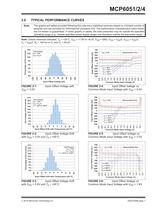
© 2010 Microchip Technology Inc. DS22182B-page 7 MCP6051/2/4 2.0 TYPICAL PERFORMANCE CURVES Note: Unless otherwise indicated, TA = +25°C, VDD = +1.8V to +6.0V, VSS = GND, VCM = VDD/2, VOUT VDD/2, VL = VDD/2, RL = 100 kÙ to VL and CL = 60 pF. FIGURE 2-1: Input Offset Voltage with VDD = 3.0V. FIGURE 2-2: Input Offset Voltage Drift with VDD = 3.0V and TA +85°C. FIGURE 2-3: Input Offset Voltage Drift with VDD = 3.0V and TA +85°C. FIGURE 2-4: Input Offset Voltage vs. Common Mode Input Voltage with VDD = 6.0V. FIGURE 2-5: Input Offset Voltage vs. Common Mode Input Voltage with VDD = 3.0V. FIGURE 2-6:...
Open the catalog to page 7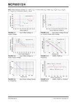
MCP6051/2/4 DS22182B-page 8 © 2010 Microchip Technology Inc. Note: Unless otherwise indicated, TA = +25°C, VDD = +1.8V to +6.0V, VSS = GND, VCM = VDD/2, VOUT VDD/2, VL = VDD/2, RL = 100 kÙ to VL and CL = 60 pF. FIGURE 2-7: Input Offset Voltage vs. Output Voltage. FIGURE 2-8: Input Offset Voltage vs. Power Supply Voltage. FIGURE 2-9: Input Noise Voltage Density vs. Frequency. FIGURE 2-10: Input Noise Voltage Density vs. Common Mode Input Voltage. FIGURE 2-11: CMRR, PSRR vs. Frequency. FIGURE 2-12: CMRR, PSRR vs. Ambient Temperature. -350 -250 -150 -50 50 150 250 350 0.0 0.5 1.0 1.5 2.0 2.5 3.0...
Open the catalog to page 8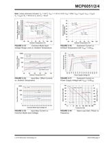
© 2010 Microchip Technology Inc. DS22182B-page 9 MCP6051/2/4 Note: Unless otherwise indicated, TA = +25°C, VDD = +1.8V to +6.0V, VSS = GND, VCM = VDD/2, VOUT VDD/2, VL = VDD/2, RL = 100 kÙ to VL and CL = 60 pF. FIGURE 2-13: Common Mode Input Voltage Range Limit vs. Ambient Temperature. FIGURE 2-14: Input Bias, Offset Currents vs. Ambient Temperature. FIGURE 2-15: Input Bias Current vs. Common Mode Input Voltage. FIGURE 2-16: Quiescent Current vs Ambient Temperature with VCM = 0.9VDD. FIGURE 2-17: Quiescent Current vs. Power Supply Voltage with VCM = 0.9VDD. FIGURE 2-18: Open-Loop Gain, Phase...
Open the catalog to page 9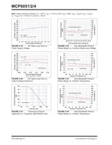
MCP6051/2/4 DS22182B-page 10 © 2010 Microchip Technology Inc. Note: Unless otherwise indicated, TA = +25°C, VDD = +1.8V to +6.0V, VSS = GND, VCM = VDD/2, VOUT VDD/2, VL = VDD/2, RL = 100 kÙ to VL and CL = 60 pF. FIGURE 2-19: DC Open-Loop Gain vs. Power Supply Voltage. FIGURE 2-20: DC Open-Loop Gain vs. Output Voltage Headroom. FIGURE 2-21: Channel-to-Channel Separation vs. Frequency (MCP6052/4 only). FIGURE 2-22: Gain Bandwidth Product, Phase Margin vs. Common Mode Input Voltage. FIGURE 2-23: Gain Bandwidth Product, Phase Margin vs. Ambient Temperature. FIGURE 2-24: Gain Bandwidth Product, Phase...
Open the catalog to page 10All Microchip Technology Inc. catalogs and technical brochures
 MicroSolutions
8 Pages
 DSA1001/3/4
22 Pages
 Embedded Computing Solutions
4 Pages
 ATmegaET128
469 Pages
 RE46C140
13 Pages
 ATmega4809
74 Pages
 16-bit MCUs and DSCs
20 Pages
 MPLAB® Harmony
12 Pages
 32-bit Microcontroller Family
20 Pages
 32-bit MPU
8 Pages
 UCS100X Family Sell Sheet
2 Pages
 PIC32 Graphics Sell Sheet
2 Pages
 PIC32 Audio Sell Sheet
2 Pages
 PIC1XF150X/155X Sell Sheet
2 Pages
 MRF24WG0MA/MB Sell Sheet
2 Pages
 MCP19111 Sell Sheet
2 Pages
 LAN9730(i) Sell Sheet
2 Pages
 Connectivity Brochure
16 Pages
 bit Embedded Control Solutions
20 Pages


Archived catalogs
 Serial Memory Products
16 Pages
 LIN J2602 Transceiver
32 Pages
 Infrared Encoder/Decoder
36 Pages
 MCP794XX I2C™ RTCC Brochure
2 Pages
 MCP1640/B/C/D
32 Pages
 Motor Control Solutions Brochure
12 Pages
 Power Management MCP1525/41
20 Pages
 PIC32 Overview Brochure
6 Pages
 8-bit PIC® Microcontrollers
16 Pages


- Liebherr signal amplifier
- Liebherr power amplifier
- Wireless module
- Potentiometer
- Liebherr compact converter
- Liebherr serial converter
- Industrial converter
- Manual potentiometer
- Crystal oscillator
- Measuring amplifier
- Liebherr voltage amplifier
- DC amplifier
- Low-noise amplifier
- Power converter
- Precision potentiometer
- Liebherr microcontroller
- Analog amplifier
- Liebherr current amplifier
- Digital converter
- Fast converter