
- Catalogs
- Master Bond
- Utilized to Bond Silicon Wafers to Glass Support Substrates during Microelectronics Fabrication


- Company
- Products
- Catalogs
- News & Trends
- Exhibitions
Utilized to Bond Silicon Wafers to Glass Support Substrates during Microelectronics Fabrication
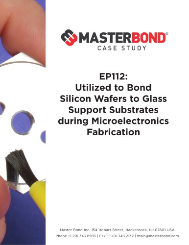
Utilized to Bond Silicon Wafers to Glass Support Substrates during Microelectronics Fabrication
Master Bond EP112 is a two-component epoxy system with ultra-low viscosity and high chemical resistance, ideal for bonding silicon wafers to glass substrates in microelectronics fabrication. It is particularly useful in processes involving high-temperature etching, ensuring substrates remain bonded.
Application #1: Bonding for Thin-Film Transfer
This application involves the START process, developed by Lawrence Livermore National Laboratory, to convert standard bulk silicon wafers into SOI-like configurations. EP112 was used to bond silicon wafers to glass substrates, facilitating the creation of a prototype liquid crystal display. The process involved curing EP112 at specific temperatures and etching in KOH to achieve desired silicon thickness. The method successfully transferred silicon circuits to glass substrates, maintaining device functionality.
Key Parameters and Requirements
- Bonding involved capillary action and curing at 110°C and 150°C.
- Etching in KOH solution at 100°C to achieve 10 µm silicon thickness.
- EP112 was chosen for its chemical resistance, optical clarity, and low viscosity.
Application #2: Wafer Thinning for Radiation Hardening
In this application, EP112 was used to bond silicon wafers to glass substrates during a novel wafer-thinning process aimed at reducing susceptibility to single-event upsets (SEUs). The process involved etching in KOH at 65°C to achieve a silicon thickness of 5–10 µm. The method maintained electrical performance of n-MOS transistors, demonstrating the effectiveness of EP112 in maintaining substrate integrity.
Key Parameters and Requirements
- EP112 was wicked into a 1 mm gap and cured at 110°C and 150°C.
- The process maintained high-quality silicon wafer surfaces.
- EP112's low viscosity and chemical resistance were critical.
Conclusions
EP112 is effective for bonding dissimilar substrates in microelectronics fabrication, offering low viscosity for easy application and high chemical resistance for maintaining strong bonds during etching processes.
Catalog excerpts
<8> M ASTERBOND CASE STUDY Utilized to Bond Silicon Wafers to Glass Support Substrates during Microelectronics Fabrication Master Bond Inc. 154 Hobart Street, Hackensack, NJ 07601 USA Phone +1.201.343.8983 | Fax +1.201.343.2132 | [email protected]
Open the catalog to page 1
CASE STUDY EP112: Utilized to Bond Silicon Wafers to Glass Support Substrates during Microelectronics Fabrication Overview of EP112 Master Bond EP112 is an ultra-low-viscosity, electrically insulating, two-component epoxy system ideal for various applications. This two-part case study series presents two use cases for EP112 for microelectronics fabrication processes when used to bond a silicon wafer to a glass substrate. Because the fabrication processes involved high temperature etching in KOH, an adhesive with high chemical resistance was required so that the pair did not de-bond during the...
Open the catalog to page 2
Results The START method combines bulk silicon's lower cost with SOI's improved device isolation and speed, thus enabling the formation of thin-film silicon microelectronics on non-silicon substrates (glass, in this case). To demonstrate the viability of using this method to transfer silicon circuits to arbitrary substrates, patterned islands were successfully transferred to a Corning® 7059 glass substrate. The transfer process maintained the surface quality of the backside of the silicon wafer after silicon thinning, ensuring it would be suitable for the final island patterning step. The authors...
Open the catalog to page 3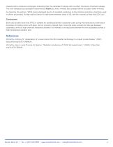
characteristics remained unchanged, indicating that the substrate thickness did not affect the device threshold voltage. This was validated by subsequent experiments (Figure 2), which showed little change before and after wafer thinning. As noted by the authors, “EP112 [was] employed due to its excellent resistance to the chemical solutions commonly used in silicon processing, its high optical clarity, its high shore hardness value of 93, and low viscosity of less than 200 cps.” Conclusions Both case studies show that EP112 is suitable for bonding dissimilar substrates used during microelectronics...
Open the catalog to page 4All Master Bond catalogs and technical brochures
 Understanding low outgassing
5 Pages


- MasterBond single-component adhesive
- MasterBond metal adhesive
- MasterBond industrial adhesive
- MasterBond plastic adhesive
- MasterBond glass adhesive
- MasterBond dispersion adhesive
- MasterBond epoxy adhesive
- MasterBond bonding adhesive
- MasterBond two-component adhesive
- MasterBond electronic adhesive
- MasterBond ceramic adhesive
- MasterBond sealing adhesive
- MasterBond fast curing adhesive
- MasterBond viscosity adhesive
- MasterBond conductivity adhesive
- Curing system
- MasterBond epoxy resin
- MasterBond rubber adhesive
- Automotive adhesive
- MasterBond composite material adhesive