
- Catalogs
- Littelfuse
- TVS Diode Array (SPA) Catalog


- Company
- Products
- Catalogs
- News & Trends
- Exhibitions
TVS Diode Array (SPA) Catalog

TVS Diode Array (SPA) Catalog
Littelfuse's TVS Diode Arrays are designed to protect signal lines from transient threats with low clamp voltage, offering enhanced protection over conventional diodes by absorbing repetitive ESD strikes without performance degradation.
- Low capacitance ranging from 30pF to 0.40pF.
- High protection levels: ESD up to ±30kV, Lightning immunity up to 150A, EFT up to 40A.
- Low clamping voltage and up to 14 inputs protection.
- Space-saving designs, RoHS compliant, Lead-Free, and Halogen-Free.
These devices protect against ESD, EMI, and Lightning by absorbing transients and clamping voltage levels, ensuring low clamp voltage during over-voltage conditions and maintaining low leakage current during normal operation.
Diagrams show the relationship between data rates, applications, and applicable Littelfuse devices, emphasizing the importance of considering capacitance in high bandwidth applications to prevent signal degradation.
The catalog lists various Littelfuse TVS Diode Arrays, detailing specifications such as working voltage, capacitance, ESD rating, and surge rating, mapping these products to suitable applications like USB ports, HDMI, Ethernet, and more.
Examples of ESD and lightning suppression implementations for different ports, including Ethernet, USB, and HDMI, illustrate the use of Littelfuse products in protecting high-speed data ports and entertainment electronics.
Littelfuse disclaims liability for errors or inaccuracies in the document and emphasizes that product specifications do not modify their terms and conditions of purchase.
Littelfuse reserves the right to modify products without prior notice. Products are not intended for life support applications unless specified, and customers assume risks for such uses.
No licenses to intellectual property rights are granted by this document. Product names may be trademarks of their respective owners.
- Operating Voltage Range: The voltage range for power supply across terminals.
- Forward Voltage Drop: Maximum voltage drop for a specific current.
- Reverse Voltage Drop: Voltage at which current begins to conduct.
- Reverse Standoff Voltage: Should be equal to or greater than peak operating voltage.
- Reverse Leakage Current: Maximum off-state leakage current.
- Clamping Voltage: Maximum voltage during peak pulse current.
- Input Leakage Current: DC current at input pins at specified voltage.
- Quiescent Supply Current: Maximum DC current at maximum voltage.
- Capacitance: Measured between input pin and reference.
Transients are short surges of electrical energy caused by energy release or induction, such as from lightning or ESD. Key characteristics include:
- Lightning: 25kV, 20kA, 10µs rise-time.
- Switching: 600V, 500A, 50µs rise-time.
- EMP: 1kV, 10A, 20ns rise-time.
- ESD: 8kV, 30A, <1ns rise-time.
Transients exhibit a "double exponential" wave. Lightning has a rise time of 1.2µs to 10µs, while ESD is less than 1.0ns.
Miniaturization increases sensitivity to electrical stresses. Microprocessors in various devices are vulnerable to transients, necessitating careful circuit design.
ESD and lightning-induced transients pose significant risks. Inductive load switching generates high-energy transients. Proper suppressor technology selection is crucial.
ESD has a rapid rise time and high peak voltages. IEC61000-4-2 standard defines ESD event models for user environments.
ESD can cause soft failures, latent defects, or catastrophic failures. Circuit protection components like Littelfuse SPA® Diodes can mitigate these risks.
ESD can cause significant damage, leading to financial losses and reputational harm. Implementing ESD suppression strategies early in design can prevent these issues.
Chip-level ESD protection involves trade-offs between protection and die space. Littelfuse offers solutions to maximize protection with minimal space usage.
Board layout is crucial in portable systems to prevent voltage overshoot from parasitic inductance, which can damage circuits. The need for board-level protection varies based on factors like board layout, IC ESD capabilities, and the potential for ESD transients to reach data lines. Empirical testing can help determine system susceptibility.
Proper circuit protection reduces ESD risks. Littelfuse TVS Diode Arrays offer low capacitance to prevent signal degradation in high-speed communications. Designers should consider potential ESD entry points and select appropriate diode arrays for protection.
ESD can enter devices through various paths, such as capacitive coupling, current injection, voltage pulses, magnetic fields, and electromagnetic fields. Identifying and fortifying weak points is essential.
Littelfuse TVS Diode Arrays provide low peak and clamping voltages for IC protection. Key considerations for suppressor selection include capacitance, peak voltage, clamping level, dynamic resistance, leakage current, standoff voltage, and the number of lines to be protected.
Manufacturers use standards like MIL-STD-883 Method 3015 and IEC61000-4-2 for testing. The MIL-STD-883 is commonly used in manufacturing, while IEC61000-4-2 is used for system-level testing. The IEC standard results in higher peak currents compared to the military standard.
Film resistors provide minimal protection and can be damaged by transients. Active components are crucial for ESD immunity, and multi-suppressor combinations can enhance protection. Preventive software programming and careful component selection are also important.
Littelfuse disclaims liability for errors or inaccuracies in the document and reserves the right to make changes without notice. Products are not intended for life support applications unless specified, and users should evaluate products for their specific applications.
The document provides technical specifications and details for the SP721 series of TVS Diode Arrays, designed for general-purpose ESD protection. These arrays are used to protect sensitive input circuits from electrostatic discharge (ESD) and over-voltage conditions.
- ESD Interface Capability: Meets MIL STD 3015.7 with 15kV and IEC 61000-4-2 standards with 4kV for direct discharge and 15kV for air discharge.
- High Peak Current Capability: ±3A for IEC 61000-4-5 (8/20µs), ±2A for 100µs pulse width, and ±5A for 4µs pulse width.
- Voltage Protection: Single-ended voltage range up to +30V and differential voltage range up to ±15V.
- Fast Switching: 2ns rise time.
- Low Input Leakages: 1nA at 25ºC typical.
- Low Input Capacitance: 3pF typical.
- Operating Temperature Range: -40ºC to 105ºC.
The SP721 is suitable for protecting microprocessor/logic inputs, data buses, and analog device inputs. It provides voltage clamping and can protect up to six external signal or bus lines.
The SP721 uses SCR/Diode bipolar structures for protection. It triggers fast at a threshold of one diode threshold above V+ or below V-. It clamps to V+ or V- when transient pulses exceed these thresholds.
The SP721's ESD capability varies with the test standard. It exceeds 15kV for air discharge and 4kV for direct discharge under IEC 61000-4-2 standards. The device can handle up to 8kV when two pins are used in parallel.
- Continuous Supply Voltage: +35V
- Forward Peak Current: ±2A for 100µs
- Maximum Storage Temperature: -65 to 150ºC
- Maximum Junction Temperature: 150ºC
- Maximum Lead Temperature: 260ºC
- Operating Voltage Range: -2 to 30V
- Forward Voltage Drop: 2V typical
- Input Leakage Current: -20 to +20nA
- Quiescent Supply Current: 50 to 200nA
- Input Capacitance: 3pF
- Input Switching Speed: 2ns
The SP721 is available in PDIP and SOIC packages. The document provides detailed dimensions and tolerances for these packages.
Details on the reflow soldering process are provided, including preheat and peak temperature conditions.
The SP721 series offers robust ESD and over-voltage protection for various electronic applications, with high peak current capability and fast response times.
- ESD Protection: Complies with IEC 61000-4-2 standards, offering 8kV direct discharge and 15kV air discharge protection. MIL-STD-3015.7 provides up to 25kV protection.
- Peak Current Capability: Handles ±7A for 8/20µs pulse and ±4A for 100µs pulse.
- Voltage Range: Single-ended up to +30V, differential up to ±15V.
- Switching Speed: Fast switching with a 2ns rise time.
- Operating Temperature: -40ºC to 105ºC.
- Microprocessor/Logic Input Protection
- Data Bus Protection
- Analog Device Input Protection
- Voltage Clamping
- Available in PDIP and SOIC packages, with lead-free and green options.
- Dimensions and tolerances are specified according to ANSI Y14.5M-1982 standards.
- Dimensions do not include mold flash or protrusions, which should not exceed specified limits.
- Lead width and terminal positions are detailed for accurate assembly and soldering.
The document outlines the specifications for a product with a lead material of copper alloy and a substitute material of silicon. The body material is molded epoxy with a flammability rating of UL 94 V-0. The lead coplanarity is specified at 0.004 inches (0.102mm).
The package dimensions are provided for Small Outline Plastic Packages (SOIC), with specific tolerances and dimensioning standards per ANSI Y14.5M-1982. Key dimensions include:
- Dimension D: 4.80 to 5.00 mm (0.1890 to 0.1968 inches), excluding mold flash and protrusions.
- Dimension E: 3.80 to 4.00 mm (0.1497 to 0.1574 inches), excluding interlead flash.
- Lead width B: Maximum 0.61 mm (0.024 inches).
Part numbers are provided with temperature ranges from -40 to 105°C, available in different package types such as 8 Ld PDIP and 8 Ld SOIC, with options for lead-free and green environmental compliance.
The SP724 series is described as a general-purpose ESD protection array, featuring:
- 4 SCR/Diode pairs in a 6-Lead SOT-23 package.
- ESD capability per IEC 61000-4-2 standards, with direct discharge up to 8kV and air discharge up to 15kV.
- Peak current capability of ±3A for IEC 61000-4-5 (8/20µs).
- Low input leakage of 1nA and low input capacitance of 3pF.
The SP724 is suitable for protecting sensitive digital or analog input circuits on data, signal, or control lines operating on power supplies up to 20VDC. It is used in microprocessor/logic input protection, data bus protection, and analog device input protection.
The document details the ESD capability of the SP724, tested to various standards including IEC 61000-4-2 and MIL-STD-3015.7. The SP724 achieves a Level 4 rating for ESD protection, with specific test conditions outlined in Table 1.
Key thermal and electrical characteristics include:
- Operating voltage range: 1 - 20V.
- Forward voltage drop: 2V at peak pulse.
- Input leakage current: -10 to 10 nA.
- Maximum junction temperature: 150°C.
The document provides soldering parameters for Pb-free assembly, with a peak temperature of 260°C and specific ramp-up and ramp-down rates.
The document includes a disclaimer noting that specifications are subject to change and that users should independently evaluate the suitability of the product for their applications.
- ESD capability up to 30kV for both direct and air discharge.
- Fast response time of less than 1ns.
- Low input capacitance of 30pF, ideal for high-speed signal line protection.
- Operating temperature range from -40ºC to 85ºC.
- Reverse standoff voltage up to 5.5V.
- Clamp voltage during ESD events up to 12V for positive and -8V for negative discharges.
- Storage temperature range from -65ºC to 150ºC.
- Diode dynamic resistance of 1.0Ω for forward conduction and 1.4Ω for reverse conduction.
- Specifications: The SP1002 series is available in SC70-3, SC70-5, and SC70-6 packages. The document provides detailed dimensions in both millimeters and inches for these packages.
- Part Numbering: The series includes part numbers SP1002-01JTG and SP1002-02JTG, indicating different channel configurations and packaging options.
- Description: Utilizes Zener diodes with silicon avalanche technology to protect I/O pins from ESD. Capable of absorbing ±30kV ESD strikes and dissipating 7A surge current.
- Features: RoHS compliant, low leakage current, and available in compact SOD723/SOD882 packages. Suitable for mobile phones, tablets, and other portable devices.
- Electrical Characteristics: Includes parameters like forward voltage drop, reverse voltage drop, and ESD withstand voltage.
- Soldering Parameters: Details on reflow conditions for Pb-free assembly, including temperature ranges and ramp rates.
- Description: Back-to-back Zener diodes for bidirectional protection, capable of withstanding ±8kV contact discharge and ±15kV air discharge.
- Features: Low capacitance, suitable for high-speed signal pins, and available in a small SOT953 package.
- Electrical Characteristics: Includes reverse voltage drop, clamp voltage, and ESD withstand voltage.
- Soldering Parameters: Similar reflow conditions as the SP1003 series.
- Disclaimer: Users should independently evaluate the suitability of the products for their applications. Littelfuse products are not designed for all applications, especially life-sustaining or life-saving applications.
- Ordering Information: Lists part numbers, package types, and minimum order quantities for each series.
- ESD protection up to ±30kV contact and air discharge.
- Low capacitance and leakage current.
- Space-efficient packaging options like 0201 Flipchip and SOD882.
- AEC-Q101 qualified for automotive applications.
- SP1007 Series: Features a bidirectional discrete TVS with a capacitance of 3.5pF and ESD withstand voltage of ±8kV (contact discharge) and ±15kV (air discharge). It operates within a temperature range of -40 to 125°C.
- SP1008 Series: Offers a bidirectional discrete TVS with a capacitance of 6pF and ESD withstand voltage of ±15kV for both contact and air discharge. It supports a peak current of 3A and operates within the same temperature range as the SP1007.
- SP1011 Series: Provides unidirectional TVS protection with a capacitance of 7pF and ESD withstand voltage of ±15kV (contact) and ±30kV (air). It is suitable for high-speed signal pins due to its low capacitance.
- RoHS compliant, halogen-free, and lead-free.
- Designed to absorb repetitive ESD strikes without performance degradation.
- Space-efficient footprints suitable for compact electronic devices.
- Maximum junction temperature is 150°C, with a maximum lead temperature of 260°C for soldering.
- Reflow conditions for Pb-free assembly include a peak temperature of 260°C with specific ramp-up and ramp-down rates.
- Package Dimensions: The SP1011 series is housed in a µDFN-6 package with dimensions of 1.25x1.0x0.5mm, compliant with JEDEC MO-229 standards.
- Soldering Parameters: Reflow conditions for Pb-free assembly include a preheat temperature range of 150°C to 200°C, with a peak temperature of 260°C not to be exceeded.
- Ordering Information: Part number SP1011-04UTG is available in a µDFN-6 package with a minimum order quantity of 3000 units.
- Description: The SD05 TVS diode is designed to replace multilayer varistors in low-speed and DC applications, providing protection against ESD and transient events.
- Features: Capable of handling ±30kV ESD strikes and 30A surge currents with low clamping voltages. It is packaged in a small SOD323 format.
- Electrical Characteristics: Includes a reverse voltage drop of 6V and a leakage current of 1.0 μA at 5V.
- Description: Similar to the SD05, the SD05C is a bidirectional TVS diode offering protection for sensitive equipment from ESD and transient events.
- Features: Handles ±30kV ESD strikes and 30A surge currents, with a low clamping voltage and packaged in SOD323.
- Electrical Characteristics: Reverse voltage drop of 6V, leakage current of 1.0 μA, and a diode capacitance of 200 pF.
- All dimensions are in millimeters and include solder plating.
- Specifications are subject to change without notice, and users should evaluate the suitability of products for their applications.
- Description: Features ultra-low capacitance rail-to-rail diodes with an additional zener diode for high-level ESD protection.
- Features: Low capacitance of 0.65pF per I/O, ESD protection up to ±8kV contact discharge and ±15kV air discharge, low leakage current of 0.5μA at 5V, and small SC70 package.
- Applications: Suitable for computer peripherals, mobile phones, PDAs, digital cameras, network hardware, test equipment, and medical equipment.
- Electrical Characteristics: Reverse standoff voltage of 6V, clamp voltage ranging from 9.5V to 13.0V, and diode capacitance between 0.35pF and 0.9pF depending on bias conditions.
- Thermal Information: Operating temperature range from -40°C to 125°C, storage temperature range from -55°C to 150°C.
- Description: Similar to SP3001 but with slightly higher capacitance and ESD protection levels.
- Features: Low capacitance of 0.85pF per I/O, ESD protection up to ±12kV contact discharge and ±15kV air discharge, and lightning protection up to 4.5A.
- Applications: Same as SP3001, with additional packaging options for space-saving.
- Electrical Characteristics: Reverse standoff voltage of 6V, clamp voltage similar to SP3001, and diode capacitance between 0.5pF and 1.25pF.
- Thermal Information: Same as SP3001.
- Package Dimensions: Detailed dimensions for SC70-6, SOT23-6, and µDFN-6 packages are provided.
- Soldering Parameters: Includes preheat and reflow conditions for Pb-free assembly with a peak temperature of 260°C.
- Ordering Information: Part numbers and packaging options for both series are listed, with a minimum order quantity of 3000 units.
- Features low capacitance ESD protection with a reverse leakage current of 1μA at 5V.
- Suitable for USB 2.0, Ethernet, HDMI, and other high-speed interfaces.
- Peak current handling of 5A and operating temperature range from -40°C to 125°C.
- Comes in a small 0402 footprint, making it ideal for compact devices like smartphones and tablets.
- Integrates low capacitance diodes with a zener diode for enhanced ESD protection.
- Handles up to 10A surge current and offers a low leakage current of 0.5μA at 5V.
- Designed for applications in Ethernet, Firewire, and flat panel displays.
- Features a small SOT23-6 package, suitable for space-constrained designs.
- Provides robust protection against ESD and high surge events, withstanding up to 20A surge current.
- Low capacitance of 4.4pF per I/O, making it suitable for high-speed signal protection.
- Applications include LCD/PD TVs, desktops, and game consoles.
- Operates within a temperature range of -40°C to 125°C.
- All series are RoHS compliant and feature lead-free assembly.
- Not intended for life support or life-saving applications.
- Specifications are subject to change, and users should verify suitability for their applications.
- Reflow soldering parameters are provided, with a peak temperature not exceeding 260°C.
- Products are available in tape and reel packaging for automated assembly processes.
- Package and Marking: The SP3304N series uses a µDFN-10 package, with a part numbering system indicating series, package type, and environmental compliance (Green).
- Product Characteristics: Features include copper alloy lead material, silicon substitute material, and molded epoxy body material with UL 94 V-0 flammability rating.
- Dimensions: Detailed dimensions are provided for the µDFN-10 package, including specific measurements in millimeters and inches.
- Description and Features: Designed to protect low voltage CMOS devices from ESD and lightning transients, the SLVU2.8 series can handle ±30kV ESD strikes and dissipate up to 40A with low clamping voltages.
- Applications: Suitable for Ethernet, WAN/LAN equipment, desktops, servers, and more.
- Electrical Characteristics: Includes parameters such as reverse standoff voltage, breakdown voltage, leakage current, and clamping voltage, with specific test conditions and ratings.
- Package Dimensions: The SOT23-3 package dimensions are detailed, along with recommended solder pad layouts.
- Description and Features: Similar to the SLVU2.8, this series offers protection with low capacitance and is suitable for high-speed data lines.
- Electrical Characteristics: Similar ratings to the SLVU2.8 series, with additional details on dynamic resistance and diode capacitance.
- Package Dimensions: The SOIC-8 package dimensions are provided, with a focus on mechanical drawings and solder pad outlines.
The document outlines the specifications for the SR05 Series TVS Diode Arrays, designed for lightning surge protection. Key features include compliance with ESD (IEC61000-4-2) up to ±30kV, EFT (IEC61000-4-4) at 80A, and lightning protection (IEC61000-4-5) at 25A. The device has a low capacitance of 6.0pF per I/O, low clamp voltage, and is packaged in a small SOT143 (JEDEC TO-253) format with a moisture sensitivity level of MSL-1.
The SR05 Series is suitable for T1/E1 IC/Secondary Protection, Ethernet 10BaseT, WAN/LAN Equipment, ISDN S/T Interface, Video Lines, and Microcontroller Input Protection.
The product is not intended for use in life support or life-saving applications unless expressly indicated.
Peak current (IPP) is 25.0A, peak pulse power (PPk) is 450W, operating temperature ranges from –40 to 125°C, and storage temperature ranges from –55 to 150°C.
Reverse stand-off voltage (VRWM) is 5.0V, reverse leakage current (IR) is 5.0 µA, reverse breakdown voltage (VBR) is 6.0V, and clamping voltage varies with current (e.g., 9.8V at 1A).
Reflow conditions for Pb-free assembly include a preheat temperature range of 150°C to 200°C, a peak temperature of 260°C, and specific ramp-up and ramp-down rates.
The part number SR05-02CTG is available in SOT143 packaging with a minimum order quantity of 3000 units.
Lead plating is matte tin, lead material is copper alloy, and the body material is molded epoxy with flammability rating UL 94 V-0.
The information is believed to be accurate and reliable, but users should independently evaluate the suitability of the product for their applications.
Catalog excerpts
Expertise Applied | Answers Delivered DIODE ARRAY Transient Voltage Suppression SPA® Diode
Open the catalog to page 1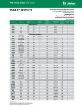
TVS Diode Arrays (SPA® Diodes) Littelfuse* Expertise Applied | Answers Delivered TVS Diode Array Technology and Applications Overview Data Protocol, Application and Product Selection Port Protection Examples Definitions and Terms Transient Voltage Threats and Scenarios ESD Suppression Strategies and Standards Legal Disclaimers © 2017 Littelfuse, Inc. Specifications, descriptions and illustrative material in this literature are as accurate as known at the time of publication, but are subject to change without notice. Visit www.littelfuse.com for m
Open the catalog to page 2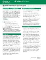
TVS Diode Arrays (SPA® Diodes) Expertise Applied | Answers Delivered Littelfuse Silicon Protection Array family of TVS Diode Arrays (SPA® Diodes) are designed to protect analog and digital signal lines, such as USB and HDMI, from various transient threats using the lowest possible clamp voltage. They offer broader application use and improved impulse protection performance over conventional diodes. These robust devices safely absorb repetitive ESD strikes at the maximum level (Level 4) specified in the IEC 61000-4-2 international standard, without performance degradation. Key Features • Low capacitance...
Open the catalog to page 3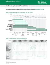
TVS Diode Arrays (SPA® Diodes) Littelfuse* Expertise Applied | Answers Delivered Data Protocol, Application and Product Selection For additional information including reference design examples, please visit www.littelfuse.com/SPA PRODUCT SERIES AND APPLICABLE DATA RATES AND PROTOCOLS Data Rate (Mbit/sec) 0 Data Protocols Typical Applications Serial Port (com) Keyboard Mouse DC Power Bus Keypad Buttons Parallel Port (LPT) Printer Scanner Coputer Input and Periperal Devices PDA / PMP / Cell Phone/ Digital Camera/ & Game Controller Ports Control System Network Hardware PCI Adapter Hub Router Webswitch...
Open the catalog to page 4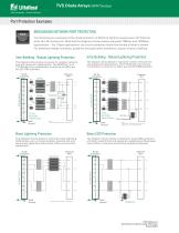
TVS Diode Arrays (SPA® Diodes) Port Protection Examples BROADBAND NETWORK PORT PROTECTION The following are examples of the implementation of ESD and lightning suppression for Ethernet ports (RJ-45 connectors). Note that the diagrams shown below represent 10Mbps and 100Mbps applications -- For 1Gbps applications, the circuit protection should be double of what is shown. For additional design examples, guidance and application assistance, please contact Littelfuse. Inter-Building - Robust Lightning Protection Intra-Building - Robust Lightning Protection The diagram show below is typical for outdoor...
Open the catalog to page 5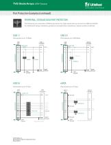
TVS Diode Arrays (SPA® Diodes) Littelfuse* Expertise Applied | Answers Delivered Port Protection Examples (continued)PERIPHERAL / STORAGE DATA PORT PROTECTION USB 1.1 The following are examples of ESD suppression for high speed data ports such as USB and eSATA. For additional design examples, guidance and application assistance, please contact Littelfuse. USB 2.0 Data speeds up to 12 Mbps Data speeds up to 480 Mbps Port Controller USB 3.0 Data speeds up to 5 Gbps * Package is shown as transparent SSTX+ SSTX-SSRX+ SSRX-Ground D+ D-Signal Ground Case Ground eSATA Data speeds up to 3 Gbps Signal...
Open the catalog to page 6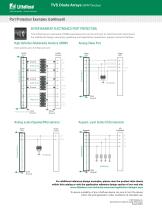
Llttelfuse* Expertise Applied | Answers Delivered TVS Diode Arrays (SPA® Diodes)Port Protection Examples (continued) ENTERTAINMENT ELECTRONICS PORT PROTECTION The following are examples of ESD suppression for ports common to entertainment electronics. For additional design examples, guidance and application assistance, please contact Littelfuse. Data speeds up to 3.4 Gbps per pair HDMI Chipset HDMI Port " Case * Package is shown as transparent Ground Video Port *— Case Ground " Signal" Ground Keypad / push button ESD protection For additional reference design examples, please view the product...
Open the catalog to page 7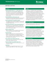
TVS Diode Arrays (SPA® Diodes) Littelfuse* Expertise Applied | Answers Delivered Definitions and Terms Liability Definitions Operating Voltage Range (VSUPPLY; SP72x Series only) The range limits of the power supply voltage that may be across the V+ and V- terminals. The SCR/Diode arrays do not have a fixed breakover or operating voltage. These devices 'float' between the input and power supply rails and thus the same device can operate at any potential within its range. Forward Voltage Drop (SP72x Series only) The maximum forward voltage drop between an input pin and respective power supply pin...
Open the catalog to page 8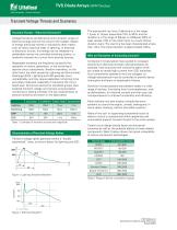
TVS Diode Arrays (SPA® Diodes) Expertise Applied | Answers Delivered Voltage Transients are defined as short duration surges of electrical energy and are the result of the sudden release of energy previously stored or induced by other means, such as heavy inductive loads or lightning. In electrical or electronic circuits, this energy can be released in a predictable manner via controlled switching actions, or randomly induced into a circuit from external sources. Repeatable transients are frequently caused by the operation of motors, generators, or the switching of reactive circuit components....
Open the catalog to page 9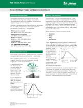
Expertise Applied | Answers Delivered Transient Voltage Threats and Scenarios (continued)Electrostatic Discharge (ESD)Inductive Load Switching Electrostatic discharge is characterized by very fast rise times and very high peak voltages and currents. This energy is the result of an imbalance of positive and negative charges between objects. ESD that is generated by everyday activities can far surpass the vulnerability threshold of standard semiconductor technologies. Following are a few examples: The switching of inductive loads generates high energy transients which increase in magnitude with...
Open the catalog to page 10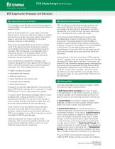
TVS Diode Arrays (SPA® Diodes) Expertise Applied | Answers Delivered It is important to consider that most electronic equipment will spend 99% of its useful life in environments where it is subject to ESD. ESD can be generated from a wide range of everyday factors such as very dry air, static from plastics, or walking across a floor or carpet, and can be present during every phase of useful life from manufacturing, to product shipping, receiving, to field handling. Electrostatic Discharge (ESD) causes millions of dollars worth of damage to electrical components, rendering circuit boards non-functional,...
Open the catalog to page 11All Littelfuse catalogs and technical brochures
 Dc Disconnect Switches
2 Pages
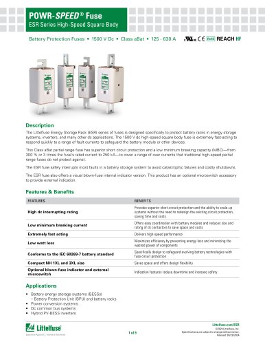 ESR_Fuse_Datasheet
9 Pages
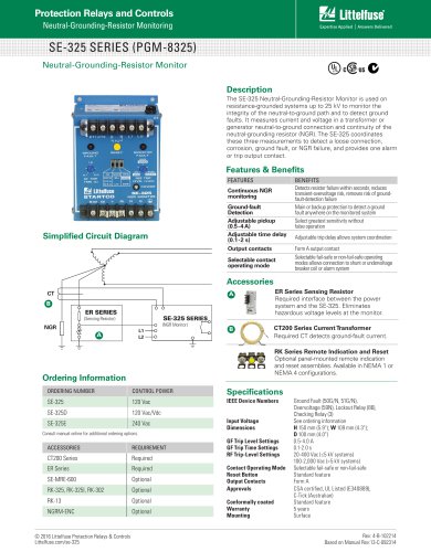 SE-325 SERIES (PGM-8325)
1 Page
 SE-CS10 SERIES
2 Pages
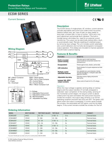 ECSW SERIES
3 Pages
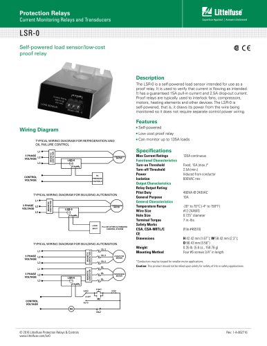 LSR-0
LSR-01 Page
 LSRU SERIES
2 Pages
 LSRX / LSRX-C SERIES
2 Pages
 50R-400-ALT
1 Page
 ALT SERIES
2 Pages
 QJxx30LH4 series
6 Pages
 Thyristors QJ8012xHx Series
8 Pages
 30KPA-HRA Series
7 Pages
 AK1-Y Series
4 Pages
 QJxx40xx Series
8 Pages
 TS Series
11 Pages
 Littelfuse SIDACtor Products Catalog
239 Pages
 Electronic Fuse Products Catalog
409 Pages
 Passenger Car Catalog
60 Pages
 Polyfuse PPTC Catalog
128 Pages
 POWRGARD Electrical Product Catalog
202 Pages
 Protection Relays SSAC Catalog
524 Pages
 Sensors Products Catalog
20 Pages
 SIDACtor Catalog
239 Pages
 Varistors Catalog
254 Pages
 SOLAR PRODUCTS CATALOG
28 Pages
 MP8000
2 Pages
 MicroPlex® SSR18 AND SSR30
2 Pages
 606 Series
3 Pages
 ST Series
3 Pages
 885 Series Fuse
3 Pages
 MicroPlex® 7X, 7H, & 7L
2 Pages
 TPSMB Series
6 Pages
 TPSMD Series
6 Pages
 ISOBUS SYSTEM
2 Pages
 POLYFUSE®
6 Pages
 Passenger Car Solutions
60 Pages
 TVS Diode Catalog
174 Pages
 Switching Thyristor Product Catalog
442 Pages



Archived catalogs
 HIGH-SPEED SEMICONDUCTOR
72 Pages
 INDUSTRIAL CIRCUIT PROTECTION
292 Pages
 Fuse Fundamentals
20 Pages
 Power Semiconductor & IC
133 Pages
 SURGE PROTECTIVE DEVICES
32 Pages
 ELECTRICAL COILS
2 Pages
 PRODUCTS FOR AGRICULTURE
36 Pages
 CIRCUIT PROTECTION
15 Pages
 MSL Classification
2 Pages
 AFTERMARKET PRODUCTS CATALOG
136 Pages
 AFTERMARKET PRODUCTS CATALOG 2018
132 Pages
 Littelfuse Thyristor Catalog
467 Pages


- Data connector
- Temperature probe
- Transformer
- Dry transformer
- Surge protector
- Resistance temperature sensor
- Proximity switch
- Level probe
- Switching relay
- Liquid level sensor
- Cylindrical proximity sensor
- Circuit breaker
- Class II surge protector
- Panel panel meter
- Protection relay
- Isolator switch
- Current transformer
- Position transducer
- IP67 proximity sensor